Evidence stage: an industrial collaboration roadmap announced by ASML and TSMC on September 8, 2026. This is neither a peer-reviewed paper nor an announcement that large-mask volume production has been completed.
#1. The conclusion in one sentence
The aim is to print smaller circuit features while increasing the area that can be transferred in one exposure. ASML and TSMC’s proposed transition to 12-inch-class photomasks changes the manufacturing ecosystem to pursue both goals together.[1]
#2. Why this problem is difficult
Think of semiconductor lithography as an exceptionally precise form of photographic printing. The wafer is the silicon substrate on which circuits are fabricated; the photomask carries the pattern to be transferred. Exposure transfers that pattern into a light-sensitive film.[3]
EUV systems use extreme-ultraviolet light with a wavelength of 13.5 nanometers. The mask and optical system reflect the light to transfer the pattern. They are not simply stencils through which light passes. The “12-inch” designation in this announcement concerns the mask format, not the wafer.[1][3]
There are two separate questions: how fine a line the system can print, and how large an area it can expose at once. These are not the same capability.
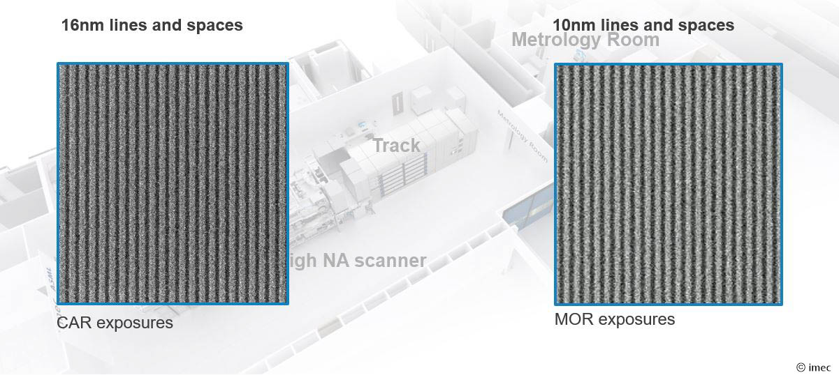
The image above comes from imec’s early High-NA material published in 2024. It shows real patterning work, but not a completed version of the large-mask system announced in 2026.
#Confusing the wafer with the mask changes the entire story
The wafer is the material on which the circuits of a finished chip are made. The mask is a tool used to transfer their pattern. Just as dough and a patterned mold serve different purposes, it matters which object is getting larger. This announcement concerns larger masks. Reading it as a change in silicon wafer size leads to very different assumptions about equipment, materials, and investment.[1]
A semiconductor is not finished after a single photographic exposure. ASML’s manufacturing guide describes coating the wafer with resist, exposing a pattern, and performing further processing to form structures. Crucially, patterns in different layers must align at their intended positions. A sharp pattern in one layer does not produce the required circuit if it is misaligned with another.[5]
Photoresist is a material that reacts to light. Rather than imagining light directly carving silicon, think of exposure as defining where later processing should occur. Lithography refers to pattern-forming technology; the exposure system transfers the pattern optically. The light source, optics, mask, and wafer motion must work together.[3][5]
#A fine brush and a large canvas solve different problems
Buying a brush capable of drawing thin lines does not make the canvas larger. A larger canvas does not sharpen the brush, either. Lithographic resolution and exposure-field size can be understood in the same way. This announcement is about extending the usefulness of precise High-NA patterning to a larger working area.
There is also a third question: speed. Even if a larger area is exposed at once, long preparation, movement, or inspection times may limit total output. Resolution, area per exposure, and hourly throughput are connected but distinct metrics. That is why this article keeps the terms separate.
#3. What was missing from the previous approach
High NA increases the numerical aperture, a quantity associated with an optical system’s ability to collect light. The NA rises from 0.33 in the existing NXE family to 0.55 in the EXE family. However, the EXE:5000, using the existing mask format, exposes a field half the size of an NXE field.[2]
A more precise tool therefore does not automatically print a wider pattern in one exposure. If a large chip does not fit within one field, separately exposed patterns must be joined accurately. This is the problem of stitching.[1][2]
#Keeping the existing mask format is itself a design choice
Retaining existing tools can reduce the scope of a technology transition. ASML explains that the EXE:5000 uses anamorphic optics, with different reduction factors in different directions, to work with conventional-size masks. The design produces a smaller exposure field than NXE systems, while faster mask and wafer stages support productivity.[2]
A stage is the mechanism that positions and moves the mask or wafer precisely. Think of a working platform with exceptionally controlled motion rather than a simple camera tripod. Concluding that output must also halve merely because the field is halved ignores other design choices. The official product description discusses the motion system for that reason.[2]
Stitching and overlay also need to be distinguished. Here, stitching means joining separately exposed areas; overlay means aligning patterns in different layers. Both demand precision, but they concern different errors. Reducing a stitching constraint does not eliminate every other alignment problem.[1][6]
#4. The new approach in three steps
First, High-NA adoption for finer patterning proceeds using the current 6-inch-class masks. High NA as a whole is not waiting for the larger mask format.[1]
Second, the companies plan the infrastructure for a later transition to 12-inch-class masks. Their stated objectives are to reduce stitching constraints and improve productivity.[1]
Third, the change must work across equipment that makes, inspects, handles, and uses the masks. This is an industrial requirement to examine, not a claim that every participating tool has already passed validation.
The established Rayleigh relationship helps explain the background physics.[4]
Here, CD is a small printable feature size, λ is the light’s wavelength, and k₁ reflects process conditions. With other conditions unchanged, a larger NA permits a smaller feature. Enlarging the mask addresses a different question: how much pattern can be held and transferred. This relationship is background theory, not an invention introduced by the announcement.
#Read the question before memorizing the symbols
The Rayleigh relationship shows which changes favor finer patterning. A smaller wavelength in the numerator and a larger numerical aperture in the denominator both help. The process factor reminds us that manufacturing conditions beyond the optics matter, too. This equation cannot by itself calculate a factory’s total cost or a finished product’s speed.[4]
For an illustrative calculation, hold wavelength and process factor constant. Changing only NA from 0.33 to 0.55 gives a feature-size ratio of 0.33/0.55, or 0.6: roughly 60% of the earlier value. This is a consequence of the simplified relationship, not a measurement from the large-mask collaboration. It does not mean chips become 40% cheaper or every circuit dimension shrinks by exactly that ratio.
A nanometer is a unit of length. EUV’s 13.5 nm refers to wavelength. Inches in the mask specification describe a tool’s size, while a manufacturer’s process-generation name has yet another context. Asking “the length of what?” is more useful than memorizing isolated numbers. Wavelength, feature size, exposure area, and mask dimensions must not be treated as interchangeable quantities.
#What a larger mask does not do for you
Even if a mask holds a larger pattern, the optics must transfer it correctly and the equipment must handle it accurately. One cannot assume that simply putting a larger mask into an existing tool delivers every expected improvement. This is why the collaboration concerns an industrial transition. Specific tool combinations and specifications require subsequent technical documentation.
In particular, the label “12-inch” is not a license to invent both lateral dimensions or a multiplier for the exposure field. Until the exact system specification is established, even a large rectangle in an illustration should be marked as an unscaled concept. Helping readers picture an object is different from providing an accurate product drawing.
#5. Key evidence and numbers
The central numbers here concern formats and schedules, not experimental accuracy. According to the joint announcement, TSMC intends to use High NA in advanced-node high-volume manufacturing from 2030. The large-mask collaboration targets a pilot line in 2031, followed by exposure-system readiness for advanced-node production in 2033.[1]
A pilot line tests repeated manufacturing and equipment integration. It should not be equated with stable volume production across an entire factory. High-NA adoption in 2030 and the large-mask system objective for 2033 are also separate milestones.
#Separate the announcement date from the initiative’s timing
The joint press release is dated September 8, 2026. It describes the initiative as established ahead of the SPIE BACUS conference on September 7. These dates need not conflict: publication and the discussion or launch of a collaboration can happen on different days. Recording both publication and event dates helps avoid counting the same development as several independent news events.[1]
The three milestones should not be collapsed into one continuous bar. The 2030 date concerns TSMC’s High-NA adoption intention; 2031 concerns the large-mask pilot line; 2033 concerns system readiness. An earlier milestone does not prove a later one has already been achieved. “Large-mask volume production is confirmed for 2030” would be stronger than the source.[1]
A pilot line validates process and equipment integration. Demonstrating feasibility there does not establish readiness to manufacture every customer’s product at the required cost and yield. High-volume manufacturing involves repeatability and operating conditions as well as scale. When the phrase appears in an announcement, first determine whether it describes an achieved result or a future intention.
An experimental paper and a company roadmap need different evaluation criteria. In a paper, we inspect controls, repetitions, and measurement conditions. Here, we ask who is participating, what they intend to prepare, and by when. Reading technical product documentation together with a customer adoption statement is appropriate. Combining them still does not produce measured performance data for a large-mask system that is not yet established.
#6. Limitations and counterarguments
Because this is a company announcement rather than a paper, demonstrated improvements must be separated from expected benefits. The joint statement does not establish a measured large-mask defect rate, hourly throughput, or cost reduction per chip.[1]
Higher productivity is a reasonable development objective, but not evidence that the objective has been met. Important questions include maintaining precision and cleanliness with a larger mask and whether gains remain after inspection and replacement costs. These are questions for subsequent validation.
#Cost is not determined by the price of one machine
A simple way to think about manufacturing cost is to compare expenditure over a period with the number of accepted chips produced. A faster machine may not increase good output as expected if defects rise. Conversely, a more expensive tool may reduce total cost by eliminating process steps or rework. This is a general framework for evaluating cost, not a claim that this announcement establishes a particular saving.
Throughput measures processing per unit time; yield measures the fraction that passes acceptance criteria. Throughput figures require exposure conditions and product context. Yield figures require a definition of failure. A company saying “productivity improves” does not imply both metrics improve by the same proportion.
A format transition also requires several participants to be ready. Mask suppliers, pattern-writing and inspection tools, storage and transport systems, and the exposure equipment must fit together. This article does not infer which supplier has won a contract or calculate related sales. A shared development direction and a concrete order disclosure are different levels of evidence.
ASML and TSMC have a direct interest in this plan succeeding. The joint announcement is meaningful evidence of customer participation, while its expected benefits still warrant scrutiny. The release itself warns that forward-looking statements do not guarantee results. There is no reason to dismiss it merely because it is corporate, or to treat the plan as an achievement merely because the companies are prominent.[1]
#7. What could actually change
If the plan succeeds, it could reduce constraints on manufacturing large chips and drive changes in mask fabrication, inspection, and transport equipment. This is an industrial interpretation, not an investment conclusion that related companies’ revenue or profits must rise.
The significance lies less in “one new machine” than in an equipment supplier and a real manufacturing customer jointly setting a transition direction. The schedule can also change if customer process choices or cost assessments change.[1]
#Development priorities may change first
Discussion of a new format leads industry participants to consider which components and inspection technologies deserve investment. Readers can interpret it as a more concrete common engineering goal rather than immediately translating it into a particular company’s sales growth. Separate official evidence is needed to connect development milestones to orders and revenue.
Constraints relevant to large-chip design may also change. But not every product needs the largest possible monolithic chip, and packaging or multi-chip integration remain part of product strategy. This article does not claim that larger masks replace every other design option. Relieving one process constraint is not the same as providing a universal industry solution.
The case illustrates that manufacturing innovation does not come from a better physical principle alone. Using high resolution in a real factory requires compatible tool formats, supply chains, inspection, and operating economics. Semiconductor news should therefore be read with an eye to the customers and manufacturing system that can adopt a technology, not only its performance table.
#8. What to watch next
The next evidence includes detailed mask specifications, actual prototypes, interoperability tests, and productivity measurements in customer processes. More decisive than a photograph of a larger mask is whether it repeatedly produces the required quality at a favorable cost.
#How to distinguish stronger follow-up evidence
Follow-up developments can be categorized as specification work, prototype demonstrations, pilot-line operation, customer process results, and repeated-production records. This is a way to classify evidence, not a prediction that every company follows an identical sequence. A prototype photograph does not establish the yield and cost performance of later stages.
Images of existing High-NA tools should be labeled as background photographs of current equipment, not presented as completed 12-inch-mask systems. Explanatory diagrams can separately show the mask and wafer, connections between exposure fields, and the three target years. Without measured performance curves, an invented cost-reduction graph would be misleading.
Finally, the apparent contradiction in the title is resolved by identifying the objects: the circuit pattern becomes smaller, while the tool carrying that pattern becomes larger. These are solutions to different problems, not opposing changes. The manufacturing-tool format is being reconsidered so that precise patterning can be used more broadly in production. That is the core development supported by this announcement.
#9. Sources
[1] ASML–TSMC joint announcement, September 8, 2026.
[2] ASML TWINSCAN EXE:5000 technical overview.
[3] ASML EUV principles and systems.
[4] ASML explanation of the Rayleigh criterion. Technical documentation accessed September 12, 2026.
[5] ASML, How microchips are made. Manufacturing background.
[6] ASML, Measuring accuracy. Alignment and metrology background.