Research cutoff — August 20, 2026, Asia/Seoul This industry map traces dependencies across the global semiconductor industry, from end markets and chip products through design, wafers and masks, FEOL/MOL/BEOL fabrication, materials, equipment and critical components, fab infrastructure, packaging, HBM and testing, to services. Companies appear in their roles as suppliers. Their inclusion carries no investment recommendation.
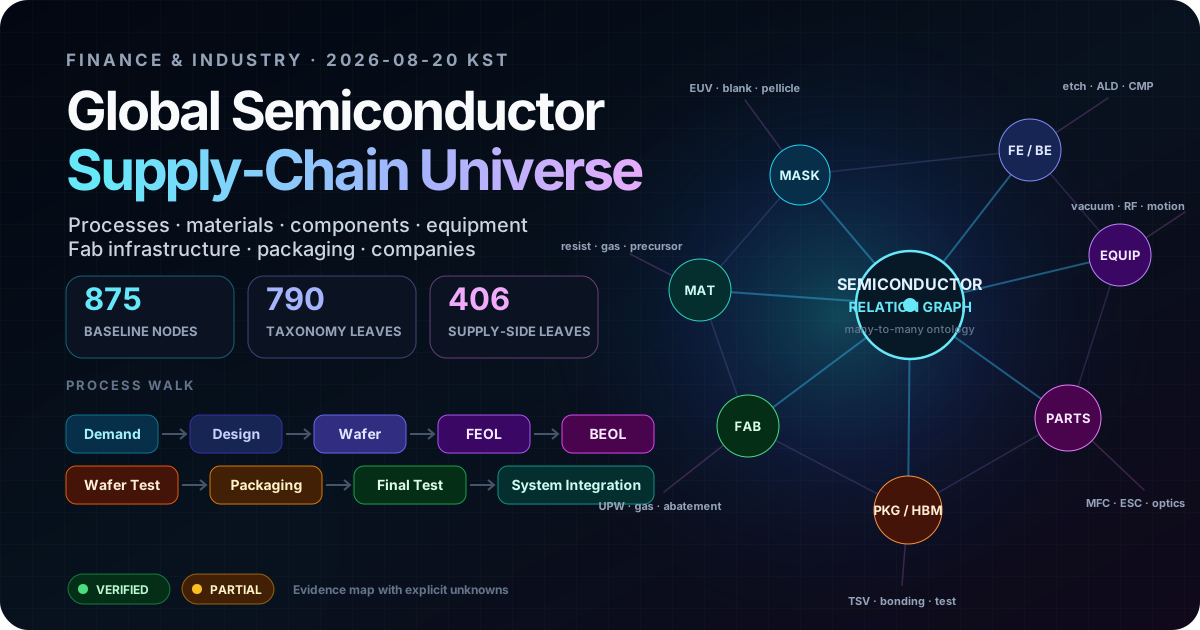
Interactive Relation Atlas
Explore the semiconductor supply chain in a full-screen Three.js / WebGPU map.
Switch among five views covering taxonomy, the manufacturing process, companies, geography and evidence. Trace dependencies upstream or downstream of nodes such as EUV, HBM, MFCs, ABF and hybrid bonding. If WebGPU is unavailable, the atlas switches to WebGL2. A 2D table and the original graph JSON are also available.
Open the interactive atlas in full screen ↗#How the semiconductor industry fits together
Looking at equipment and materials suppliers in isolation misses how demand reaches them. Increased AI server demand first changes the specifications and quantities of GPUs, HBM and networking chips. This creates new requirements for design, masks, advanced processes, wafer starts, packaging and testing. Only then does it translate into specific demand for lithography, etch, deposition and inspection tools, gases, chemicals, vacuum systems, RF power, substrates, automation and service.
The map first connects five layers, then places companies where they actually supply a product or service.
| Layer | Question to ask | What to look for |
|---|---|---|
| Demand and products | Where is demand changing across AI, mobile, automotive and industrial markets? | Specifications and volumes for logic, memory, power devices and sensors |
| Design and manufacturing technology | Which process nodes, architectures, masks and levels of process complexity does the product require? | Wafer starts, number of process steps, mask layers and yield learning |
| Capacity and operations | Who is adding fab or back-end capacity, where and when? | Capacity, utilization, tool installations and service demand |
| Equipment, materials and critical components | Which subsystems limit quality, yield or throughput? | Lithography, etch, deposition and inspection tools, gases, chemicals, RF, vacuum and thermal control |
| Packaging, testing and risk | How are dies connected and verified? Which supply interruptions would delay the product? | Advanced packaging, HBM, substrates, testing, qualification and geography |
Major industry suppliers describe similar connections in their public materials. TSMC’s foundry ecosystem extends from logic wafer manufacturing to mask making, packaging and testing. ASML’s lithography offering includes computational lithography, metrology, system integration and service for its installed base. KLA describes process control as a way to protect yield across wafers, reticles and advanced packaging. TSMC annual reports · ASML 2025 Annual Report · KLA 2025 Annual Report
A two-minute guide for first-time readers
The names of companies, tools and process steps can be overwhelming at first. Start with a single chip. What has to happen to make it, and which tools, materials and components have to work together at each step?
Three questions are enough to begin.
- What are we making? HBM for an AI server, an application processor for a smartphone and a power semiconductor for a car each require different structures and processes.
- What changes on the wafer? Deposition adds a film, lithography transfers a pattern, etching removes selected material and chemical mechanical planarization (CMP) flattens the surface. These operations recur across layers.
- What keeps the result repeatable? A tool relies on gases and chemicals, vacuum pumps, RF power, temperature control, sensors, robots, consumables and maintenance.
Follow the chain from end demand → chip structure → wafer processes → equipment subsystems → materials and components → verification and service. A company’s place in the chain becomes clear once you can identify the product, technology or service it supplies.
#Start with one etcher
Imagine a circuit pattern is already on a wafer. An etcher selectively removes unwanted film to turn the pattern into lines, holes and walls. Inside the tool, a robot and equipment front end module (EFEM) handle the wafer. An electrostatic chuck (ESC) and chiller control temperature, a mass flow controller (MFC) meters gas, an RF source and matching network sustain the plasma, a vacuum pump removes byproducts and a sensor detects the endpoint.
Changing the MFC or pump can change the process result. Once you can trace those dependencies in an etcher, you can read a deposition tool, CMP tool, scanner or metrology system in the same way. Start at Etch in the interactive map
#Follow one wafer through the industry
Starting with company names encourages shortcuts such as “ASML means lithography” or “Lam means etch.” Follow a wafer instead and the reasons these companies interact come into focus. Volume manufacturing repeats these steps tens or hundreds of times, with inspection and cleaning between them.
Demand and chip design → masks and patterning → film formation → etching and structure formation → measurement and yield learning → volume manufacturing → packaging and test
#1. Demand and chip design establish what to make
AI servers, smartphones, cars and industrial equipment create different kinds of semiconductor demand. An AI accelerator needs compute dies, HBM and high-speed package interconnects. Automotive power semiconductors require high-voltage, high-reliability materials and lengthy qualification. The product determines circuit architecture, process node, wafer count and packaging method.
Design companies and integrated device manufacturers (IDMs) turn requirements into circuits. The design must satisfy manufacturing rules, be transferred to masks and have a viable path to production yield. Foundries such as TSMC work at that junction. TSMC’s Foundry 2.0 definition spans mask making, packaging and testing as well as wafer fabrication. TSMC 2025 Annual Report
#2. Patterning transfers a circuit design to the wafer with light
Patterning transfers one circuit layer onto a wafer. Light projects the mask pattern onto photoresist. After development, the resist that remains guides the next step. The idea resembles printing a stamp, but as linewidths shrink, diffraction, mask errors, wafer positioning and distortion from earlier processes can all affect the result.
ASML supplies the scanner for this step. Achieving the target linewidth and alignment between layers (overlay) repeatedly and at production speed also takes computational lithography, masks, resist, pellicles, overlay metrology, and service and upgrades after installation. ASML 2025 Annual Report
#3. Deposition adds material for the next structure
Circuits are built from many thin, uniform films, including insulators, metal interconnects, barriers and transistor layers. Chemical vapor deposition (CVD) forms films through gas-phase precursors and chemical reactions. Physical vapor deposition (PVD) transfers material physically. Atomic layer deposition (ALD) uses sequential surface reactions. The choice affects thickness uniformity, interface quality and conformality, or how evenly a film covers the inside of a fine structure.
Applied Materials supplies a wide range of tools for controlling materials, surfaces and interfaces. Customers ask whether a deposited material will survive subsequent etching and meet the device’s electrical requirements. Film quality depends on the precursor, gas, MFC, showerhead, heater, plasma and RF systems, vacuum and abatement, which is why all appear as dependencies. Applied Materials process portfolio
#4. Etching removes selected film to form walls, holes and channels
Once the film and resist pattern are in place, etching removes exposed material. It forms structures such as transistor gates, contact holes for interconnects and deep holes in 3D NAND. This is how a two-dimensional pattern becomes a three-dimensional device feature.
Lam Research and Applied Materials are major suppliers of etch tools. In dry etching, RF power creates a plasma. Reactive species and ions selectively remove the target material. Small changes in gas distribution, RF power, vacuum, temperature, the ESC or the edge ring can alter depth, profile and uniformity. More complex NAND stacks and 3D logic thus place greater demands on chambers, RF systems, vacuum and gas delivery as well as on the overall etcher. Lam’s introduction to plasma etching
#5. Measurement feeds each step back into yield improvement
Patterning, deposition and etching recur over many layers. A small defect or an error in thickness, linewidth or overlay can go through several costly steps before anyone finds it. Inspection locates defects. Metrology measures quantities such as linewidth, film thickness and overlay.
KLA is a major supplier in process control. Its tools provide data to identify which tool, recipe or material condition needs to change to restore yield. This feedback matters in mask production and advanced packaging as well as in wafer fabrication. KLA FY2025 Annual Report
#6. Volume manufacturing and packaging turn a working die into a system component
A fab repeats these processes reliably at scale. Foundries such as TSMC manage wafer starts, process operations, yield stabilization and shipments for customers’ designs. Capacity depends on qualified tools working together, skilled operators, utilities, suppliers, service and actual utilization as well as physical space.
Once the wafer is finished, individual dies must be separated, connected to a substrate, cooled and electrically tested. For HBM and chiplets, connections among dies within a package can determine performance and constrain supply. TSMC includes advanced packaging in its foundry ecosystem, and KLA supplies package inspection and metrology. A die becomes a usable system component after packaging and testing.
#Where the companies fit
TSMC connects design, fab operations and advanced packaging. ASML supplies the patterning systems that reproduce circuit layouts accurately. Applied Materials has a broad role in films and materials. Lam supplies etch, deposition and cleaning tools for complex structures. KLA measures the results and feeds them back into yield improvement. Each name now identifies a supplier or operator along the wafer’s route.
#What the map establishes
The unit of analysis is a leaf node with a distinct procurement market, qualification process or unit-process function. Each leaf is linked to a manufacturing step and, where supported, to the companies that supply it.
Phase 1 established a baseline of 875 nodes and 790 leaf nodes. Phase 2 reorganized the supply-side leaves covered directly by the supplier census into 406 nodes. Market shares, customer qualifications and high-volume manufacturing (HVM) supply by Korean companies still require verification for individual nodes.
The public atlas records two things side by side.
- Taxonomy topology shows where an item belongs and which processes, tools, materials and components it connects to.
- Evidence status marks sufficiently corroborated information as
VERIFIEDand partially established information asPARTIAL. Unconfirmed customer relationships and market shares are left open.
This page is the public interface to a semiconductor research database that accumulates evidence as it becomes available.
#Why the map uses a graph
A supplier can participate in several categories of the semiconductor supply chain. A tree that assigns each company to one category would lose those relationships.
Applied Materials spans ALD, CVD, PVD and electrochemical deposition (ECD), as well as etch, CMP, implantation, metrology, photomasks, hybrid bonding and compound and power semiconductors. ASML connects scanners with computational lithography, metrology and inspection. Korea’s FST spans pellicles, EUV pellicle handling and inspection, SiC chamber parts, scrubbers and chillers.
The database therefore allows these many-to-many relationships.
Supplier ↔ Material / Equipment / Component / Service
Equipment ↔ Subsystem / Consumable / Utility
Process ↔ Material / Equipment / Metrology / Software
Device architecture ↔ Process intensity
End market ↔ Product demand ↔ Manufacturing demand
These links preserve distinctions obscured by treating ASML as synonymous with exposure tools, outsourcing assembly and test (OSAT) as synonymous with packaging, or the materials and components sector as a handful of large equipment companies.
#1. Which parts of the semiconductor supply chain are on the map?
The map places every industrial layer involved in moving a semiconductor from demand through design, fabrication, packaging and qualification into a system. Demand on the left sets specifications and volumes. Design, wafers and processes in the middle create the die. Packaging and test on the right turn it into a usable component. Materials, equipment, critical components, fab infrastructure and automation support the entire flow.
| Industry layer | Scope | Question to ask |
|---|---|---|
| Demand and products | DEM covers AI/HPC, servers, mobile and automotive. PROD covers DRAM, HBM, NAND, CPUs, GPUs, power devices and sensors. | Who needs which chips, and in what quantity? |
| Design, substrates and masks | DESIGN covers IDMs, fabless firms, foundries, EDA and IP. WAF covers silicon, SOI, SiC, GaN and epitaxy. MASK covers blanks, reticles, pellicles and inspection. | What pattern and starting material does the chip require? |
| Wafer fabrication and process control | FE covers cleaning, lithography, etch, deposition, implantation, CMP and metallization. PC covers inspection, overlay, critical dimension (CD), yield and advanced process control (APC). | How is the structure formed on the wafer, and how is it checked? |
| Materials, equipment and critical components | MAT covers resists, gases, chemicals, precursors, CMP and chamber materials. EQCOMP covers vacuum, RF, gas delivery, chambers, motion, optics, thermal systems, robotics and sensors. | Which consumables and tool subsystems change the process outcome? |
| Fab operations | FAB covers cleanrooms, ultrapure water (UPW), gases, chemicals, abatement, cooling and power. AUTO covers AMHS, FOUPs, MES, FDC, APC and cybersecurity. | What does it take to process thousands of wafers repeatedly under the same clean conditions? |
| Finishing, verification and reuse | PKG covers thinning, bump formation, TCB, hybrid bonding, RDL and TSVs. TEST covers probing, ATE, burn-in and reliability. HBM and SERVICE are also included. | How are chips connected, protected and qualified, and how is equipment maintained and restored? |
#2. Follow a wafer through manufacturing
To connect the taxonomy to an actual manufacturing sequence, imagine following a single wafer through the factory.
| Stage | What happens to the wafer or die | Related supply chain |
|---|---|---|
| 1. Starting material | Silicon, SiC or GaN is made into a high-purity wafer. | Ingots, epitaxy, polishing, cleaning and substrate inspection |
| 2. Pattern preparation | Circuit design data is transferred to a reticle. | EDA, mask blanks, writers, pellicles and mask inspection |
| 3. Wafer fabrication | Films are deposited, patterns are printed with light and selected regions are etched to form transistors and interconnects. | Deposition, lithography, etch, implantation and CMP, plus gases, resists, vacuum, RF and metrology |
| 4. Wafer test | Electrical testing identifies candidates for known-good dies (KGD). | Probe cards, testers, inspection and yield analysis |
| 5. Packaging | The wafer is thinned and diced. Dies are connected to other dies and protected. | Dicing, substrates, bumps, TCB, hybrid bonding, molding and thermal management |
| 6. Final verification and system integration | Finished components are checked for performance and reliability and installed in server, mobile or automotive systems. | ATE, handlers, burn-in, sockets, system-level test (SLT) and reliability |
The sequence in brief runs from demand → chip specifications → design and masks → wafer fabrication → wafer test → packaging → final test → system. Materials, equipment, critical components and fab infrastructure recur at every transition.
At each step, the analysis asks about ten inputs and functions.
- Equipment
- Material
- Consumable
- Critical component
- Gas / chemical
- Contamination control
- Metrology / inspection
- Wafer handling
- Utility / facility
- Maintenance / service
This approach gives several activities their own nodes even though a conventional overview of the major wafer processes can overlook them. These include post-etch cleaning, edge and bevel processing, descum, temporary bonding and debonding, inline chemical and gas analysis, carrier cleaning, calibration and refurbishment.
#3. Critical components inside a process tool
A map that starts with equipment manufacturers can overlook the critical subsystems inside their tools.
The etcher illustrates how to read the table. The same questions apply to scanners, deposition tools, CMP systems and cleaning tools.
| Etcher subsystem | Representative components | Process function | Consequences of instability |
|---|---|---|---|
| Reaction space | Chamber body, liner, coating, quartz, ceramics, SiC and seals | Contains the reaction and protects internal surfaces. | Particles, corrosion and process variation |
| Plasma and power | Plasma source, RF generator, matching network and power supply | Generates reactive plasma and delivers stable power. | Poorer etch profiles and repeatability |
| Holding and temperature control | ESC, electrode, edge or focus ring, chiller and heater | Holds the wafer in position at a controlled temperature. | Nonuniformity between the wafer center and edge |
| Gas delivery | Purifier, regulator, valve, MFC and showerhead | Controls purity, pressure, flow and distribution. | Changes in reaction chemistry and uniformity |
| Vacuum and exhaust | Dry pump, turbopump and gauge | Maintains pressure and removes byproducts. | Poor pressure response, contamination and residual byproducts |
| Handling and automation | Load port, EFEM and robot | Moves wafers precisely while controlling contamination. | Particles, misalignment and loss of throughput |
Worked example: How an etcher shapes a device
#What does an etcher do?
An etcher selectively removes unwanted parts of a thin film already deposited on a wafer. Think of a sculptor carving stone along the outline left by a developed photograph. An exposure tool transfers the pattern with light. The etcher then turns the pattern into a three-dimensional structure. Samsung’s introduction to etching · Applied Materials etch overview
In dry etching, gas enters a vacuum chamber and RF power creates a plasma. Radicals react chemically with the material, while ions deliver energy toward the wafer and help etch the bottoms of features. The vacuum system removes volatile reaction products. The etcher coordinates gas delivery, electric fields, temperature, pressure and wafer handling to obtain the desired profile. Lam Research on plasma chemistry and ion bombardment
#Five steps inside the tool
-
Load the wafer using the robot, EFEM and load port
The tool removes the wafer from its front-opening unified pod (FOUP), moves it inside and aligns its orientation and position. Even slight contamination or misalignment at this stage can cause defects later. EFEM, load port and robot examples
-
Clamp the wafer and set its temperature with the ESC, edge ring and chiller
An electrostatic chuck (ESC) holds the wafer in place with electrostatic force. Backside helium and a chiller remove heat to stabilize its temperature. Temperature changes can alter both etch rate and sidewall profile. How an ESC works · Semiconductor chiller example
-
Meter the gas through the purifier, regulator, valve, MFC and showerhead
The purifier reduces impurities, the regulator and valve control pressure and flow, and the mass flow controller (MFC) meters the gas. The showerhead distributes it across the wafer. Even with identical gas chemistry, variations in flow and distribution can produce different results at the center and edge. MFC product overview
-
Etch selected regions using the plasma source, RF generator and matching network
The RF generator supplies power, and the matching network adjusts for the chamber’s electrical load so power transfers efficiently. Ions and radicals in the resulting plasma remove material exposed by the mask. Alongside etch rate, engineers track directionality (how straight the feature is), selectivity (how well other films survive) and uniformity across the wafer. RF power and matching networks
-
Remove byproducts and check the endpoint with chamber liners, coatings, pumps, gauges and sensors
Chamber walls and liners withstand plasma exposure, resist corrosion and control particles. Dry pumps, turbopumps and valves manage pressure and exhaust. Sensors help identify the moment the target film has been removed. Even a single component replacement can require rechecking particles, pressure response, RF conditions and yield. Semiconductor dry pumps · Endpoint monitoring example
#How the components form a supply chain
The components form a feedback loop through gas delivery → plasma generation → wafer reaction → byproduct removal → sensor feedback. MFC drift can change gas composition, plasma and RF conditions, and the etch profile. An unstable ESC or chiller changes wafer temperature, affecting selectivity and uniformity. Degraded pumps, valves or liners can alter pressure or contamination enough to change the result of the same recipe.
Open the Etch process in the interactive map, then select MFC, Plasma / RF, ESC, Vacuum Pump and Robot / EFEM in turn. Each node links to official technical resources.
#Inside a scanner
A scanner uses light to transfer a circuit pattern to a wafer. Its source generates the required wavelength, and precision optics direct the light. Stages move the reticle and wafer, while encoders measure their positions. Vibration isolation prevents tiny movements from becoming pattern errors. Handling systems transport reticles and wafers cleanly. Sensors and overlay metrology check how well the new layer lines up with the preceding one.
The scanner supply chain thus extends from light sources and lenses to precision motion, position encoders, vibration control, reticle pods and handling, wafer stages and overlay measurement. A small layer shift can cause faulty connections or yield loss after many layers have been built up.
#Inside a deposition tool
A deposition tool builds thin films of metals, insulators, barriers or liners to a specified thickness and uniformity. The delivery system supplies precursors. A vaporizer converts liquid precursors to vapor, and MFCs, valves and a showerhead control the amount and distribution. A heater sets the reaction temperature. Some processes use plasma and RF to enhance reactivity. Pumps remove unused gas and byproducts, and abatement equipment treats hazardous exhaust.
Performance depends on uniformity across the wafer, coverage inside narrow and deep structures, and control of particles and impurities. As in an etcher, gas delivery, thermal control, vacuum, plasma and chamber materials operate as one connected system.
#Why requalification is a barrier to entry
Replacing a component in a semiconductor tool can change particle generation, plasma uniformity, thermal stability, outgassing, corrosion resistance, RF impedance and pressure response. These checks all lead to one practical question. After the replacement, does the wafer still have the same feature geometry and electrical characteristics?
Tool suppliers and fabs therefore requalify the equipment and validate wafer yield. They first check that tool conditions remain repeatable, then examine actual wafers for defects, dimensions, electrical characteristics and yield against prior levels. This takes time, and recipes vary by customer. The installed base, qualification time and local service network are consequently barriers to entry. A supplier must be able to replace and qualify its component reliably across tools already running in the field.
#The chemistry behind semiconductor materials
Broad material categories conceal differences that matter in procurement and qualification.
- Lithography: KrF/ArF/ArFi/EUV resist, developer, thinner, BARC, topcoat, HMDS, EBR chemical
- Wet processes use H₂SO₄, H₂O₂, HF, HNO₃, HCl, H₃PO₄, NH₃, IPA and other ultrahigh-purity solvents.
- Etch/clean gases: fluorocarbon, chlorine, bromine, NF₃, F₂, remote-plasma clean chemistry
- Deposition: ALD/CVD metal·high-k·barrier/liner precursor, carrier/purge gas
- Implantation and doping use dopant gases or sources based on boron, phosphorus and arsenic.
- CMP: slurry, pad, conditioner, post-CMP clean chemistry
- Plating: Cu chemistry, suppressor, accelerator, leveler, electroless chemistry
- Chamber consumables: quartz, alumina, AlN, Y₂O₃ coating, SiC, graphite, elastomer seals
- Packaging: ABF, BT resin, EMC, underfill, NCF/NCP, die attach, TIM, flux, solder/bump materials
Even substances with the same chemical name can form distinct qualification markets. Semiconductor-grade metal impurities, particles, moisture, delivery stability and the cleanliness of containers and valves all matter.
#How HBM connects multiple manufacturing processes
The HBM supply chain spans the following steps.
AI accelerator demand
→ Advanced DRAM wafer
→ Wafer test / Known Good Die
→ TSV etch + liner/barrier/seed + Cu plating + CMP
→ Wafer thinning / stress relief / reveal
→ Microbumps and Cu pillars or a hybrid interface
→ High-accuracy placement + TCB / bonding
→ MR-MUF·NCF·molding
→ Logic base die + interposer/RDL + package substrate
→ TIM / heat spreader / warpage control
→ Final test / burn-in / high-speed thermal test
HBM4 brings more I/O, a logic base die and greater stack and package complexity. Thermal management, power integrity and testing become more demanding as bandwidth rises. To trace how HBM demand reaches suppliers, follow the chain below.
AI server
→ GPU / accelerator shipments and HBM bytes per accelerator
→ Advanced DRAM wafer demand
→ TSV / thinning / bonding step intensity
→ Interposer / substrate / thermal complexity
→ Probe / KGD / package test value per package
→ Equipment, material, component and service revenue exposure
HBM4 mass production, HBM4E sampling or qualification and a future HBM roadmap describe distinct stages. Whether hybrid bonding is in production must be established for each HBM4 product.
#How technology changes reach the supply chain
#GAA / Nanosheet
Three-dimensional gate and channel geometries increase the intensity of conformal ALD, selective epitaxy, selective or isotropic etch, interface control and 3D metrology.
#Backside Power Delivery
Backside power delivery changes front-side routing and adds dependencies on temporary bonding, extreme thinning, backside alignment, via etching, dielectric and metal deposition, lithography, CMP and backside inspection.
#High-NA EUV
High-NA EUV qualification links the scanner’s source, optics and stages to masks, pellicles, resists and underlayers, track defectivity, stochastic defect control, overlay and actinic inspection.
#Hybrid Bonding
As bond pitch shrinks, tolerances on surface roughness and planarity tighten. CMP, ultraclean surface preparation, plasma activation, submicron alignment, interface metrology and known-good dies become more important.
#Chiplet / UCIe
More dies and die-to-die interfaces make package co-design, RDLs, interposers and substrates, placement and bonding, signal and power integrity validation, and partitioned testing more complex.
#SiC / GaN
Substrate defects, epitaxial quality, high-temperature processes, backside metallization, wafer handling and specialized inspection give SiC and GaN their own process flows, distinct from silicon CMOS.
#Structural chokepoints
Where public sources did not establish current market shares at the node level, the map leaves them open. Candidate chokepoints are identified through supplier concentration, qualification requirements, replacement time, technical barriers and geographic concentration.
| Chokepoint family | Why a bottleneck can form |
|---|---|
| EUV and High-NA scanners, optics and sources | Demanding integration of optics, light sources and motion systems, a limited supplier base and lengthy joint qualification |
| Advanced mask ecosystem | EUV blanks, multibeam writing, blank and actinic inspection, and pellicles depend on one another. |
| Leading-edge process control | Shrinking defects and 3D structures make inspection and metrology essential to yield learning. |
| ABF and high-end substrates | Rising package density, long qualification and complex build-up substrate processes |
| ATE, probing and high-speed test interfaces | Higher AI and HBM I/O counts and power increase demands on test coverage, signal integrity and temperature control together. |
| Critical tool components | Replacing MFCs, valves, purifiers, RF systems, ESCs, pumps or abatement equipment can trigger tool and process requalification. |
| Ultrahigh-purity chemistry | A contamination event can cause yield losses across multiple lots. |
#South Korea’s semiconductor supply chain
Beyond memory manufacturing, Korea has a substantial supplier base in silicon wafers, specialty gases, selected photoresists and process chemicals, dry stripping, deposition and cleaning, high-pressure annealing, scrubbers and chillers, cleanrooms and fan filter units (FFUs), chamber consumables, FCBGA substrates and test interfaces.
The availability of a domestically produced component establishes one milestone. Qualification for leading-edge high-volume manufacturing requires additional evidence.
| Node | Assessment as of August 20, 2026 |
|---|---|
| Silicon and selected SiC wafers | Capable of competing globally |
| DUV resists, wet chemicals, NF₃ and WF₆ | Suppliers compete domestically and globally. |
| Selected deposition, cleaning, dry-strip and high-pressure annealing tools | Competitive capabilities, with gaps that vary by node |
| Quartz, silicon and SiC chamber parts | Domestic suppliers can compete across much of the category. |
| Scrubbers, chillers, cleanrooms, FFUs and AMHS | Strong domestic ecosystem |
| FCBGA substrates, sockets, pins and test interfaces | Globally competitive suppliers in selected nodes |
| EUV scanners and High-NA optics and sources | Effective import chokepoints |
| Advanced mask blanks and actinic inspection | High reliance on overseas suppliers |
| Leading optical and electron-beam process control | High reliance on overseas suppliers |
| Leading-edge ion implantation and high-end ATE | High reliance on overseas suppliers |
| ABF | Very high reliance on overseas suppliers |
| Hybrid bonding | Development and qualification stages vary by application. |
A survey limited to listed companies misses smaller and specialized suppliers. FST, Value Engineering, Seojin Electron, DeviceEng, CanTops, LSE, SUNJE, MMT, MMP, 3SLINE, Gauss Labs, Woowon Technology and Semics merit follow-up in individual leaves such as components, carrier cleaning, AMHS interfaces, utility monitoring, technical representation and wafer test. Exhibitor listings and product pages establish that a product exists. Confirming supply to a Samsung Electronics or SK hynix HVM line requires official evidence of the customer relationship. Until then, the relationship remains UNVERIFIED.
#Regional strengths
| Region | Main areas of strength |
|---|---|
| United States | EDA/IP, deposition/etch/implant, process control, ATE, AI compute |
| Korea | DRAM/HBM/NAND, memory HVM, specialty gases·chemicals, selected equipment/components/test |
| Taiwan | leading foundry, advanced packaging, substrate ecosystem |
| Japan | wafer, resist, mask blank, high-purity chemicals, CMP, clean, dicing/test equipment |
| Netherlands | lithography, deposition, advanced bonding |
| Germany | EUV optics/laser, specialty materials/equipment |
| France | industrial/specialty gases, SOI ecosystem |
| China | Mature-node expansion, intensive development of domestic alternatives and exposure to advanced-tool export controls |
| Singapore / Malaysia / Vietnam | supplier manufacturing hubs, OSAT/test, downstream electronics·packaging expansion |
| India | Design talent and expansion of fab and assembly, testing, marking and packaging (ATMP) capacity |
| Israel | specialty process, metrology/inspection R&D |
The country where equipment is made and the country hosting the fab where it is delivered are separate geographic dimensions.
#Market size and the scope of each estimate
A market figure needs a definition and a reference period.
| Metric | Data period | Status | Value |
|---|---|---|---|
| Semiconductor equipment billings | 2025 | Actual | $135B |
| Total semiconductor manufacturing equipment | 2026 | Forecast | $165.9B |
| Wafer Fab Equipment | 2026 | Forecast | $143.9B |
| Test equipment | 2026 | Forecast | $15.3B |
| Assembly / packaging equipment | 2026 | Forecast | $6.7B |
| Semiconductor materials | 2025 | Actual | $73.2B |
| Wafer-fab materials | 2025 | Actual | $45.8B |
| Packaging materials | 2025 | Actual | $27.4B |
| Semiconductor device market | 2026 | Forecast | $1.51T |
The device market in the last row measures chip sales. Equipment and materials cover different transactions, so adding their addressable markets to chip sales would misstate the size of the overall semiconductor market. Fab equipment spending and equipment billings also use different definitions.
#Evidence discipline
The map distinguishes the following stages of a customer relationship.
Rumor
→ Evaluation
→ Sample shipment
→ Qualification
→ Production qualification
→ Initial mass production
→ High-volume manufacturing
→ Long-term supply agreement
An expected shipment to Samsung Electronics and a confirmed supply relationship with a Samsung volume production line are different claims. The relationship remains UNVERIFIED without confirmation in official customer or supplier materials, disclosures or contracts.
Individual claims also carry an evidence grade.
- A: Primary source + independent corroboration
- B: Primary source only
- C: High-quality secondary source
- D: Company marketing claim only
- E: Rumor / weak evidence
The map excludes grades D and E as support for its principal conclusions.
#Current coverage and open questions
The interactive atlas includes the audited topology, major process nodes, dependencies among tools and components, representative global and Korean suppliers and selected customer relationships confirmed by official sources. The public graph currently renders 322 nodes and 611 relationships.
The following remain PARTIAL or UNKNOWN.
- Current global supplier shares for all 790 leaf nodes
- The 2025 and 2026 addressable market and compound annual growth rate for each detailed market
- Customer-specific evaluation, qualification and HVM stages for smaller Korean suppliers
- Coverage of domestic replacements in China at the level of individual leaves
- High-NA production adoption by foundry and by layer
- The bonding process of record for each HBM generation
- Complete many-to-many revenue mapping at the legal-entity and subsidiary level
Keeping those gaps visible is a condition of the map’s research quality.
#Using the interactive atlas
- Taxonomy lens shows the hierarchy of 15 top-level domains and their child nodes.
- Process lens orders nodes by the wafer’s route through manufacturing.
- Company lens organizes the graph around suppliers, buyers and platforms.
- Geography lens shows regional supply-chain strengths and geographic dependencies.
- Evidence lens distinguishes VERIFIED and PARTIAL status and the evidence grades.
- Incoming / Outgoing trace highlights upstream and downstream relationships for the selected node.
- Search jumps to a node ID, process, material, component or company name.
- 2D table searches the same graph without a GPU.
#Primary source registry
The following primary sources underpin the market estimates, technology status and taxonomy in this public edition.
- SEMI — Semiconductor Equipment Market Data
- SEMI — 2025 Semiconductor Materials Market, $73.2B
- SEMI — Semiconductor Components, Instruments and Subsystems
- SEMICON Korea — Exhibitor and category structure
- WSTS — 2026 global semiconductor market forecast
- ASML — High-NA EUV readiness milestone
- Intel Foundry — Intel 18A, RibbonFET and PowerVia
- SK hynix — HBM4 development and mass-production readiness
- Micron — HBM4 high-volume production
- U.S. BIS — Export-control changes for foreign-owned fabs in China
- Korean Ministry of Trade, Industry and Energy — notices on semiconductor materials, components and equipment, mini-fabs and advanced packaging
#Priorities for the next update
The map is a versioned research resource. Three changes take priority in the next update.
- Connect the 790 leaf nodes and 406 supply-side leaves directly to a machine-readable ledger.
- Require every supplier–customer edge to specify its evaluation, qualification or HVM stage and source date.
- Expand the source registry to distinguish market definition, total addressable market, and actual, estimated or forecast values for each node.
The goal is to record what is known, which relationships have been verified and where further investigation should begin, while keeping unresolved questions visible.