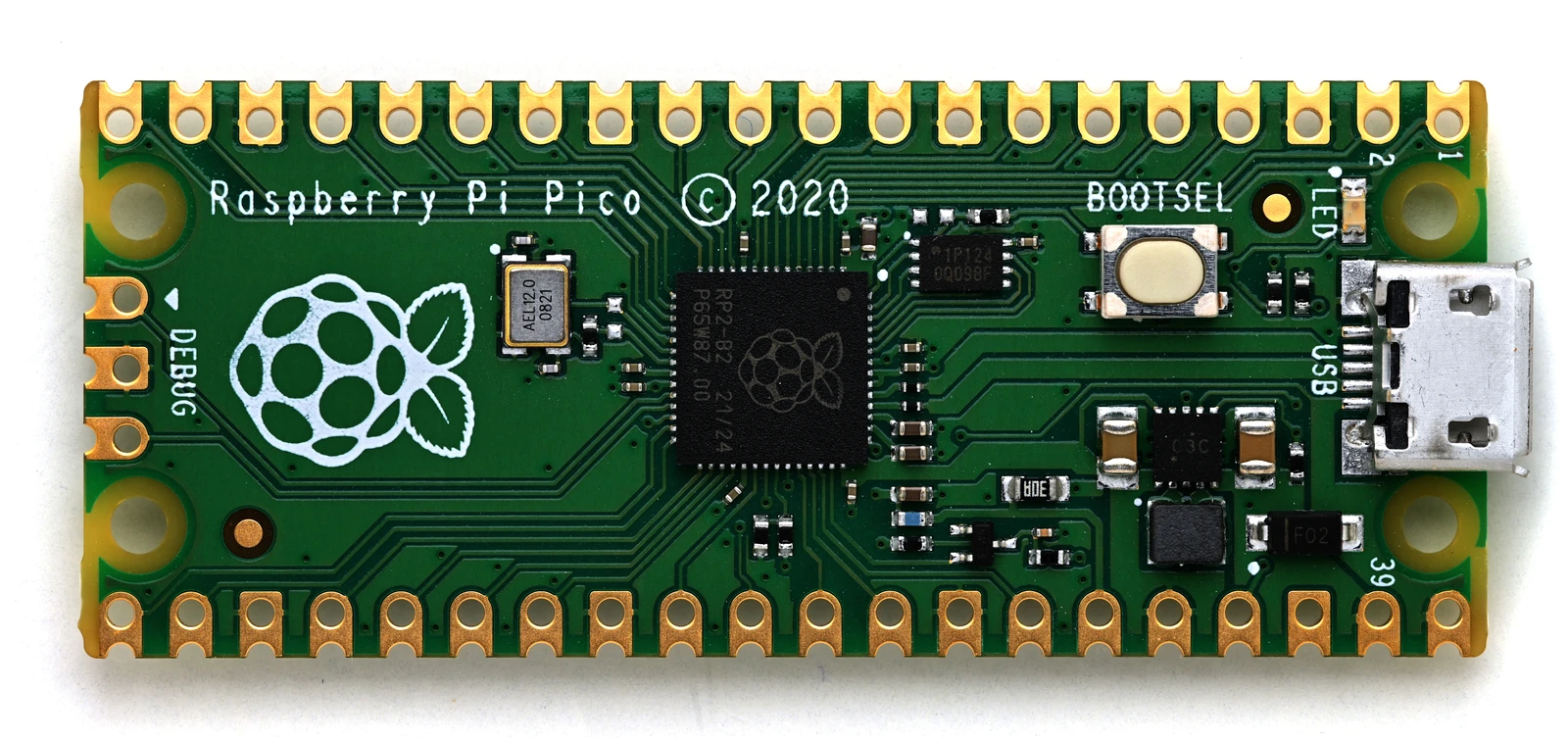
Is the whole green board a CPU? Or is the black chip in the middle the CPU? Start with a real Raspberry Pi Pico photograph, then open the manufacturer’s datasheet for the same RP2040. Identify the physical board, the chip package and the internal CPU cores before memorising the terms.[4][19][20]
The board, chip and CPU are not the same object.
 View full image ↗
 Pico is the board. RP2040 is the chip. Cortex-M0+ is a core inside it.
LOOK IN THIS ORDER
- The whole green boardThis is the Raspberry Pi Pico board, containing a chip, USB connector and other components.
- The black square near the centreThis is the RP2040 MCU package. It contains CPU cores and other circuits.
- Where are the CPU cores?They are not visible on the package surface. Locate the two Cortex-M0+ cores in the next datasheet figure.
A call to read_sensor() returns a number. But the operation remains unexplained unless we identify the circuit communicating with the sensor, the space holding its data, the condition notifying the CPU, and the address and meaning of a read. A CPU executes instructions; an SoC, or System-on-Chip, integrates multiple system functions in one integrated circuit.[1][2]
Learning goals: distinguish a CPU from the complete chip, draw the path of a sample, and explain the specification that hardware, software and verification engineers must share. You do not need to write C to follow this chapter. Later lessons will supply the detailed foundations of addresses and bits.
The evidence baseline is 2026-09-28. Documented product examples are separated from an invented educational design. The real photograph and the manufacturer’s original Figure 2 come first; five separate teaching diagrams simplify the ideas. Photographs, source figures and invented examples are clearly distinguished, and functional diagrams are not physical die layouts or measured waveforms. This chapter implements no RTL, device driver or OS port and makes no claim of measured hardware performance.
#1. SoC, CPU, MCU, ASIC and FPGA: relationships and different classification axes
#Why does lining up the names cause confusion?
These terms all concern chips, but they classify different things. CPU → MCU → SoC → FPGA is not a hierarchy of size or performance. The table is an educational synthesis of official definitions and actual products, not a mutually exclusive universal classification standard.[1][2][3][4][5][6][7]
| Term | Focus | Starting point |
|---|---|---|
| CPU, Central Processing Unit | Instruction execution | A processing element that reads program instructions and performs computation and control. |
| ISA, Instruction Set Architecture | Instruction and behavior rules | Specifies the instructions software can use and their meaning; it is not a particular CPU circuit. |
| MCU, Microcontroller Unit | An integrated control device | A microcontroller combining a CPU core, memory, peripherals and related functions. |
| SoC, System-on-Chip | Integration of system functions | Combines processing, memory and input/output functions on a chip, without requiring every external component to be built in. |
| ASIC, Application-Specific Integrated Circuit | A chip designed for a particular purpose | An integrated circuit designed and manufactured for the required functions and application. |
| FPGA, Field-Programmable Gate Array | Configurable logic and connectivity | Configuration data establishes logic functions and connections to implement hardware behavior. |
RISC-V is an ISA specification. A CPU core implementing it and a complete chip containing that core are separate objects. Therefore, sharing an ISA does not by itself make sensor addresses, peripherals or drivers identical. This is an inference from the distinction between instruction rules and concrete device implementation.[3][9][11]
#Check the boundaries against real chips
Raspberry Pi’s RP2040 contains two Arm Cortex-M0+ cores, 264kB of internal SRAM, and peripherals including SPI, I²C and UART. It uses external QSPI flash. Cortex-M0+ is a core; RP2040 is an MCU containing those cores. The RP2040 chip must also be distinguished from a board carrying it. This documented example is enough to reject the claim that every MCU necessarily contains internal flash.[4]
AMD’s Zynq 7000 SoC combines Arm processors and FPGA programmable logic. That is why asking whether something is an SoC or an FPGA is not always an exclusive either/or choice.[7]
Configuring FPGA logic and connections operates at a different level from executing CPU instructions. Similarly, describing an ASIC’s circuit as fixed should not be expanded into a claim that no software or settings on that chip can change. Identify which part is configurable and which part executes instructions.[5][6][7]
#2. The roles of CPU, memory, interconnect, peripherals and accelerators
A fast CPU does not make the external-signal interface or storage space disappear. Separating the problem each block solves makes the system structure visible. The roles below reconstruct the SoC overview, an actual MCU configuration and AMBA documentation for beginners; they are not a mandatory block list for every product.[1][2][4][8]
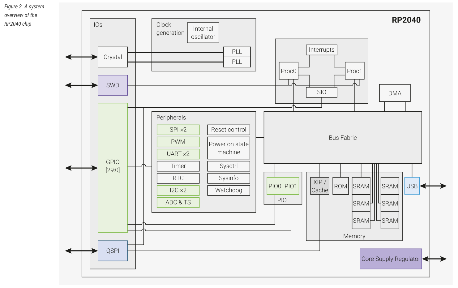
The photograph showed the outside of the package. Now look at the official functional structure of that same RP2040. In the manufacturer’s Figure 2, read Proc0/Proc1 at upper right, then Bus Fabric, SRAM and Peripherals. You do not need to memorise every block.[20]
Read inside the chip using the manufacturer’s diagram.
 View full image ↗
 The CPUs are two blocks within this system—not the whole system.
LOOK IN THIS ORDER
- Proc0 / Proc1Upper right: first locate the two processor cores that execute instructions.
- Bus FabricThe large middle box: connections that carry requests and data between cores, memory and peripherals.
- Memory / SRAMLower right: internal memory that can hold working data or code.
- PeripheralsMiddle left: communication hardware such as SPI, UART and I²C exists alongside the CPU cores.
| Block | Why is it needed? | Role in the sensor example |
|---|---|---|
| CPU core | Instructions and decisions need somewhere to execute. | Read sensor values and evaluate conditions. |
| Memory | Working data and code need storage. | Hold acquired samples and computed results. |
| Peripheral controller | Communication rules must match the external device. | Communicate with the sensor through an interface such as SPI. |
| Interconnect | Address requests and responses need a delivery path. | Connect CPU requests to the correct memory or device. |
| Clock, reset and pin circuitry | Timing, initial state and external connections need preparation. | Start acquisition under defined conditions. |
| Accelerator, optional | Selected processing can be assigned to a separate circuit. | Add filtering when required; not included in this minimal design. |
FROM CODE TO CHIP · 00
↕ External communication
Illustrative SoC boundary · not a physical die layout
Shared support: clock · reset · pin configuration · IRQ delivery
External memory and its controller can be added when required. SoC does not mean that every component must be on-chip.
In Figure 1, distinguish the external sensor from the acquisition circuitry inside the chip. The central path connecting the CPU, SRAM and peripherals is the interconnect. Specific connection rules can use standards such as AMBA, Advanced Microcontroller Bus Architecture. AMBA connects and manages SoC functional blocks; its individual interfaces address different requirements. Detailed AXI signal rules and NoC topologies are outside this chapter.[8]
In this context, IP, Intellectual Property, denotes a design block integrated into the system, not an Internet address. Thinking in terms of CPU cores and peripheral controllers also reveals the distinction between designing a block and connecting existing blocks.[1]
Our first design question is not whether to attach an NPU, but what data must be retained, at what rate and for how long. That is the teaching approach for this series. We do not define GPU, NPU, DDR or Linux as mandatory merely because a device is called an SoC.
#3. How one sensor sample reaches an application
#Trace data and notification separately
We now define an invented educational system containing an external digital sensor, an SPI acquisition controller, a sensor_fifo IP, a CPU and SRAM. The acquisition controller supplies already-acquired unsigned 16-bit samples to the FIFO. We are not modeling SPI electrical signaling or framing. Acquisition and interrupts are disabled immediately after reset.
Once acquisition is enabled, incoming samples enter a FIFO, or First-In, First-Out buffer: the oldest item is retrieved first. When the data interrupt is enabled and the FIFO is nonempty, a service request to the CPU stays asserted. In this example, IRQ, Interrupt Request, carries no sample payload. Software checks the status and separately reads the data register to obtain a sample.
FROM CODE TO CHIP · 00
- AcquireThe acquisition controller obtains a 16-bit sample.
- BufferInsert into the FIFO. Drop the new sample when full.
- NotifyHold data IRQ while the FIFO is nonempty and its interrupt is enabled.
- ReadSoftware checks STATUS; one successful DATA read consumes one sample.
- UseCode running on the CPU stores and processes the returned value.
In this example IRQ carries no sample payload. This is an ordering diagram, not a time-scaled or measured waveform.
A driver is not another circuit beside the CPU doing independent computation. It is software running on the CPU. Linux provides a common device, bus and driver model, as well as IIO, Industrial I/O, for sensor categories. A real system can separate the sensor driver from the SPI-controller driver. None of this means our invented IP is already supported by Linux, Zephyr or AUTOSAR. A bare-metal exercise may instead process the value in a function without an operating-system layer.[12][16]
#Registers specify behavior shared by hardware and software
We use MMIO, Memory-Mapped I/O, as the interface through which the CPU accesses the device. Knowing an address is not enough. Width, bit meanings, initial state, permitted accesses, read/write side effects and invalid-access results must be defined. OpenTitan’s regtool is a real example of generating register documentation, RTL and C headers from a shared specification. It distinguishes access semantics including read-only, read-clear and write-one-to-clear.[9]
The following table is a limited contract for our example, not a real chip. Addresses are offsets relative to the invented IP’s base, not physical addresses to access on your computer. Software may perform only aligned, full-word 32-bit accesses. The FIFO contains 16 entries.
| Offset | Name | Access, reset state and behavior |
|---|---|---|
0x00 | CTRL | RW. bit0 ENABLE=0. Writing 1 enables acquisition of subsequent samples. Clearing it does not empty the existing FIFO. |
0x04 | STATUS | RO, with no read side effect. Initially bit0 EMPTY=1, bit1 FULL=0 and bits12:8 COUNT=0. |
0x08 | DATA | RO with a pop side effect on a successful read. Return the oldest 16-bit sample zero-extended to 32 bits and remove one item. Reading an empty FIFO returns an error and removes nothing. |
0x0C | IRQ_ENABLE | RW. bit0 DATA_READY, bit1 OVERFLOW. Both initially 0. |
0x10 | ERROR | bit0 OVERFLOW, W1C. Initially 0; becomes 1 when a new sample is dropped because the FIFO is full. With no new event, writing 1 clears it and writing 0 leaves it unchanged. |
Reserved bits read as zero and ignore writes. Writes to RO registers, undefined offsets, unaligned accesses and partial-word accesses return an error without changing state. The actual bus encoding of that error will be specified after a protocol is selected in a later lesson.
A complete reset initializes the FIFO, configuration and error state. Inputs while ENABLE=0 are outside acquisition. When enabled but full, the FIFO preserves existing items and uses a drop-new policy. The data interrupt is active when the FIFO is nonempty and its enable is set; the overflow interrupt is active when ERROR and its enable are both set. IRQ remains active if either condition holds, so clearing ERROR can leave a data IRQ active.
We also separate out the educational rule for simultaneous events. Reset has highest priority. Otherwise, a valid read/pop of existing data is applied before assessing space for the incoming sample. If a new overflow event coincides with a W1C write, the new event wins and the error remains set. The hand-worked exercises below avoid simultaneous events. Do not generalize this chosen priority to unrelated IP.
FROM CODE TO CHIP · 00
Educational ERROR.bit0 = 1 · no new error event
Addresses and bits belong to the illustrative contract in the text. Common generation can reduce disagreement but cannot eliminate errors in the specification itself.
A shared specification is a starting point for reducing hardware/software disagreement. But if the original specification is wrong, generated implementations can share that error. Reviewing requirements and independently derived expected results is the second message of Figure 3. Actual Linux access code must follow the applicable MMIO contract, including __iomem, ioremap(), readl() and writel(). Here we refer to the concepts in the Linux 6.18 documentation and execute no kernel code.[9][11]
#Failure case: writing zero does not clear the error
Educational situation: ERROR.bit0=1 and no new inputs arrive. The data interrupt is disabled and only the overflow interrupt is enabled. Writing zero as though ERROR were a normal variable leaves both the error bit and the overflow IRQ set. W1C, Write One to Clear, requires writing one to clear the bit. Under these conditions, writing one to that bit clears both.
As a real documented example, OpenTitan’s FROM CODE TO CHIP · 00 Educational IRQ_STATE.OVERFLOW · same clock edge OpenTitan is a real example that specifies simultaneous HW/SW updates. The priority shown here is a choice of this educational DUT.earlgrey_1.0.0 UART specifies INTR_STATE.rx_overflow as rw1c. That is a field in the actual UART. The offset and bit0 of our ERROR register are invented. Keep the documented access meaning separate from the educational address.[9][10]\n\n
#Failure case: adding a log consumes a sample
Educational situation: the FIFO contains 0x0011 followed by 0x0022. If code reads DATA once to print a log, then reads it again for processing, the first access returns 0x0011 and the second returns 0x0022. Unless the first result was retained, logging has consumed that sample.
The solution under this contract is to read the device once, store the returned value in a software variable, and use that variable for both logging and processing. Two STATUS reads consume no samples; two DATA reads consume two. Read-only, RO, does not mean that reading leaves all state unchanged. The pop behavior is defined by our invented contract, while the existence of access side effects is established by official register documentation.[9]
#4. Specification → model → RTL → implementation → bring-up → verification
#What do you produce and hand to the next engineer?
Having written a design and having collected evidence of its behavior are different states. OpenTitan tracks hardware-design and hardware-verification stages separately. Accordingly, we do not portray verification as something performed only once at the end.[13]
| Stage | Input | Educational handoff artifact | Question to answer |
|---|---|---|---|
| Requirements | Sensor type, sample rate, latency and loss policy | requirements.md | What counts as success or failure? |
| Architecture and interfaces | Requirements and candidate blocks | Block diagram, address map and register specification | What connects, under which rules? |
| High-level model | Functional and traffic assumptions | Behavior model and assumption list | Can buffering tolerate delayed service? |
| RTL and testbench | Interface and state rules | Hardware description, stimuli and oracle | Do normal operation, reset, full buffers and concurrent accesses follow the contract? |
| FPGA or ASIC implementation | RTL and constraints | Bitstream or synthesis/physical-implementation outputs | Does the selected implementation meet its constraints? |
| Bring-up and software integration | Board/chip and initialization procedure | Boot, register and interrupt observations | What is the first path that actually works? |
| Regression and defect closure | Tests, failures and changes | Reproduction logs, verification scope and exclusions | What has been rechecked after the change? |
This is an educational handoff flow, not a claim that these filenames or roles are a particular company’s standard. Its foundations are the ASIC overview, OpenTitan development stages and SystemC, OpenROAD and Linux documentation.[6][13][14][15][16]
FROM CODE TO CHIP · 00
At every stage: requirements ↔ implementation ↔ test evidence ↔ correction and retest
An educational handoff map, not a company organization chart or mandatory lifecycle. An FPGA observation is not complete ASIC verification.
SystemC is used for C++-based system modeling, design and verification, supporting hardware/software partitioning and architecture exploration. Not every project must use SystemC, and not every model is synthesizable. After RTL, Register-Transfer Level, describes state and data movement, synthesis and physical implementation remain separate, target-dependent activities.[6][14][15]
Reading one sample during bring-up observes the basic path under those conditions. It does not establish that boundary inputs, reset, overflow, simultaneous accesses and timing have all been verified. Do not extend success on an FPGA into success across all ASIC physical conditions. Record what was checked and under which conditions.[6][13][15]
#5. Artifacts shared by circuit, verification, firmware and driver engineers
The table maps the nine original job items to educational roles in the invented sensor system. Actual responsibilities must be checked against the company’s product, team and tools.
| Job item | Question in this example | Example artifact |
|---|---|---|
| Arm/RISC-V core-based design and verification | Which memory, reset and interrupts connect to the CPU? | CPU-subsystem specification and integration tests |
| Bus architecture design and verification | Does an address request reach the correct block? | Address map, connectivity and traffic/error tests |
| High-level and detailed digital IP design | How are acquisition, storage, full-buffer behavior and status implemented? | Functional model, register specification and RTL |
| FPGA prototyping | Does the design operate on the board while meeting constraints? | Project, constraints, bitstream and observations |
| Device-driver design | How is the device initialized and data delivered under OS rules? | Driver, synchronization, error handling and API tests |
| MCAL design | How is MCU-dependent access separated from upper-level functionality? | Module configuration, API implementation/integration and register mapping |
| OS porting | How is the execution environment prepared for the CPU, SoC and board? | Startup code, board description, port configuration and boot evidence |
| Test software design | Are the required samples and states actually observed? | Inputs, independent expected results, verdict rules and logs |
| Static/Dynamic Coverage verification | What has been checked and what remains? | Applied methods, coverage and uncovered/excluded items |
MCAL, Microcontroller Abstraction Layer, handles MCU-dependent peripheral access and reduces hardware dependencies in higher layers. An ordinary driver is not automatically an AUTOSAR-compliant implementation. OS porting also needs to distinguish a new CPU-architecture port, SoC support and board support. Zephyr provides separate guides for those three layers.[17][18]
The exact company-specific meanings of NIC and Static/Dynamic Coverage remain unknown. Without the company, target IP, analysis tools and responsibility boundaries, we do not assign a single definitive interpretation. This chapter teaches relationships between concepts; it does not certify the responsibilities in a particular job advertisement.
#6. The common example and separate practice environments
#Calculate service delay and sample loss without a board
This exercise is specification reading and hand tracing. No board, compiler, RTL simulator or target OS is used, and no concrete ISA has been selected. On paper or in an editor, produce system-map.md, register-contract.md, handoff-map.md and test-plan.md, or use four sections of one document.
Assumptions: at t=0 the FIFO is empty, its depth is 16 and ENABLE=1. At t=1, 2, …, 20ms, one sample with values 1, 2, …, 20 arrives. No reads occur through the completion of the input at 20ms. Incoming items are dropped when full. There is no intervening initialization, simultaneous read or additional reset.
Work out the retained values, discarded values and error bit just after 20ms, then open the answer.
COUNT=16. Values 1–16 are retained and 17–20 are discarded. ERROR.bit0=1. Conservation is generated 20 = stored 16 + consumed 0 + dropped 4. Payload storage is 16 × 16 ÷ 8 = 32 bytes, and payload input rate is 1,000 × 2 = 2,000 bytes/s. These calculations exclude metadata, circuit resources and transfer overhead.
Even a small input data rate can overflow a buffer when reads are delayed long enough. Here the issue is maximum service delay relative to finite storage, not the CPU’s peak computation rate. Twenty slots would cover the stated interval, but initial occupancy, bursts, longer delays and subsequent consumption rate are needed to size a real device. These are calculations under assumptions, not RTL or OS simulation results or measured throughput.
The second task disables the data IRQ, enables only the overflow IRQ and writes zero then one to ERROR, with no new input. The third resets the device, inserts two samples and compares two STATUS reads with two DATA reads. The fourth assigns an input, a modified artifact and an output to each of the nine job items. Use the preceding specification to judge the answers, without presenting an expected result as a real board log.
RTL/FPGA, Linux, RTOS and MCAL exercises will choose supported targets and versions separately in later lessons. Do not assume that the same imaginary device or source code runs unchanged across them. What we complete here is a map for understanding, not a chip with certified behavior.
#Three misconceptions and five review questions
Misconception 1: SoC is another name for CPU. A CPU executes instructions, whereas SoC describes system integration. Misconception 2: the same ISA implies the same sensor driver. Instruction rules do not fix device addresses and access semantics. Misconception 3: reading a read-only register cannot change state. Our DATA contract forbids writes while still defining a read side effect.[1][2][3][9]
Must two chips using the same RISC-V ISA use the same sensor driver?
An ISA specifies instruction execution. It does not make peripheral addresses, access side effects or the OS device model identical. ISA identity alone therefore cannot establish driver identity.[3][9][11]
Does an MCU always contain internal flash?
No. RP2040 is a documented MCU example using external flash.[4]
If an ERROR bit remains one after writing zero, is the circuit defective?
Not under our contract. With no new error, writing one clears the W1C bit. On a real device, first inspect the specification for that field.[9][10]
What remains when 20 samples enter a 16-entry FIFO without reads?
Given an initially empty FIFO, the stated time boundary and drop-new policy, 16 samples remain, four are dropped and OVERFLOW is set. Saying that the CPU is fast does not eliminate a service gap.
What has been verified after reading one sample on an FPGA, and what remains?
The basic path has been observed under those conditions. Reset, full buffers, concurrent accesses, long runs and timing may need separate verification. ASIC physical conditions remain a separate matter.[6][13][15]
Chapter conclusion: circuitry acquires and stores data; software reads it under defined rules; verification links those rules to observed results. The next learning topic is the foundation needed to describe this behavior over time: combinational and sequential logic, clocks, registers and addresses. That follow-up chapter has not yet been published.
#References and evidence boundaries
The research date is 2026-09-28. The entries below identify the overview or specific sections checked in the preceding research, not validation of entire documents or complete product behavior. MMIO and IIO references retain Linux 6.18 paths; the UART example retains earlgrey_1.0.0. Master/latest documents refer to the research snapshot. Product examples apply only to those products; invented addresses, FIFO/IRQ policies and calculations apply only to the educational contract above. No scores, performance guarantees or inferred company-specific responsibilities are claimed.
[1] Arm, What is SoC Development?, definition, components and development overview.
[2] Arm, What is a CPU?, definition and instruction-execution role.
[3] RISC-V International, Ratified Specifications, specification overview used to distinguish ISA from implementation. No individual extension version selected.
[4] Raspberry Pi, Microcontroller chips, RP2040 features.
[5] Arm, What is FPGA?, overview of configurable logic and interconnect.
[6] Arm, What is an ASIC?, definition and design process.
[7] AMD, Zynq 7000 SoCs, processor and programmable-logic integration example.
[8] Arm, AMBA, overview and principal specifications. No individual AXI/APB version selected.
[9] OpenTitan, reggen & regtool: Register Generator, Register Tool, input format and swaccess table.
[10] OpenTitan, UART Registers, earlgrey_1.0.0, INTR_STATE.rx_overflow.
[11] Linux, Bus-Independent Device Accesses, 6.18, device access, __iomem and access functions.
[12] Linux, Industrial I/O Introduction, 6.18, sensor categories and SPI/I²C examples.
[13] OpenTitan, Hardware Development Stages, separate design and verification progress. Project-specific criteria are not universal industry thresholds.
[14] Accellera/SystemC, SystemC overview, C++-based modeling and HW/SW partitioning. Not a full-standard review or an executed synthesis-tool qualification.
[15] OpenROAD, Documentation, RTL-to-GDSII physical-implementation overview. The tools were not run.
[16] Linux, The Linux Kernel Device Model, devices, buses and drivers. The header’s initial date of 2002-08-26 and update of 2006-01-31 are not used to establish current API examples.
[17] Zephyr, Porting, separation of architecture, SoC and board guides. No specific port implemented.
[18] Renesas, Microcontroller Abstraction Layer (MCAL), peripheral access and upper-layer abstraction overview. Not an AUTOSAR compliance verdict.
[19] Phiarc, Raspberry Pi Pico top.jpg, 2023-03-18, CC BY-SA 4.0. Real photograph, resized and converted to WebP.
[20] Raspberry Pi Ltd, RP2040 Datasheet, build 3184e62-clean, 2025-02-20, §1.2–1.3, Figure 2, printed p.10 / PDF page 11. CC BY-ND 4.0. Unchanged figure excerpt. Functional structure, not a physical die layout.