Begin with the practical idea. The switches inside computer chips can be made with extremely thin channel materials. This study grew a single atomic layer of boron, carbon and nitrogen—BCN—over a wafer-scale area, fabricated multiple p-type transistors, and measured their electrical behavior. Its importance lies in connecting the atomic arrangement of a monolayer material with functioning devices in one investigation. It does not mean the entire wafer has become a commercially qualified chip, or that complete complementary CMOS circuits combining p-type and n-type devices have entered mass production.[1][2]

#Why show this photograph, and what does it not show?
The photograph shows repeated circuit patterns on an actual silicon chip wafer. It is a background illustration of what it means to fabricate many devices on one substrate. It is not a photograph of the BCN wafer or a microscopy image from this study. The BCN paper’s Figures 1 and 2 contain growth and atomic-resolution images, but the publisher’s public page does not provide a confirmed Creative Commons reuse permission for those figures. Readers can consult the paper’s original figure list and the University of Tokyo research team’s explanation. This article does not reproduce original figures whose reuse rights have not been established.[1][2]
Start here New to wafers, transistors or p-type materials? Open the explanation
A wafer is a thin substrate on which semiconductor devices are made. Repeating fabrication over a relatively large surface lets researchers investigate process uniformity more meaningfully than making only one or two devices. The phrase wafer-scale describes the area over which material is formed. By itself, it does not establish that every device at every location has the same quality, or that every portion of the wafer is ready to become a saleable chip.
A transistor is an electrical switch that controls a current path. Charge entering through the source travels along a thin channel toward the drain. Voltage applied to the gate regulates how readily current can pass through that channel. In this paper, BCN is the channel material. For a further explanation of source, gate and drain, the site also has a beginner introduction to MoS₂ transistors, currently in Korean. That link is an explicitly identified Korean original, not a claimed English translation.
In a p-type channel, current is described primarily in terms of the motion of holes, which behave as positively charged carriers. An n-type device primarily uses electron transport. CMOS combines complementary types to implement logic. Demonstrating a promising p-type material is therefore a different milestone from showing that p-type and n-type devices can be jointly fabricated and operated as a complete circuit on one wafer.
#What is BCN, and how should we picture its structure?
Hexagonal boron nitride, BN, can be pictured as a thin honeycomb-like crystal containing boron and nitrogen. In the investigated B–C–N monolayer, carbon atoms or carbon pairs occupy some positions in that lattice. The paper describes carbon substituting preferentially at nitrogen sites and producing local lattice distortion. This is not the same physical picture as sprinkling carbon powder over an intact BN layer, or simply mixing a sheet of graphene with BN. Atomic arrangement and electronic structure change together; the authors report and interpret an approximately 1.90 eV bandgap in the resulting material.[1]
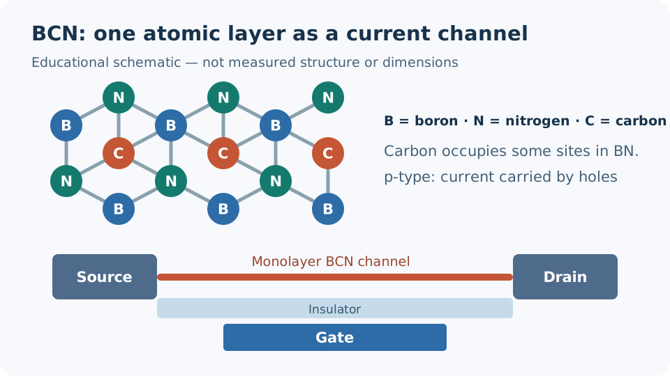
The upper portion of the illustration simplifies only the concept of carbon entering a B–N network. The lower portion is an educational schematic showing a BCN channel and the different roles of source, drain and gate. It does not reconstruct the actual distribution or fraction of carbon atoms, the electrode geometry, a measured cross-section, the paper’s 20 nm HfO₂ layer thickness, or any experimental performance curve. For actual atomic-resolution observations and device drawings, readers should use the paper’s Figures 2 and 5. The English version changes the educational diagram’s labels, not its status as an illustration rather than experimental evidence.[1]
Nor does “monolayer” automatically mean a perfectly smooth and uniform surface, like an idealized sheet of paper. The University of Tokyo account reports cross-sectional observations supporting a monolayer and an AFM step height of approximately 0.5 nm. An AFM step-height measurement depends on the substrate and measurement conditions; it should not be restated as “the exact diameter of one atom is 0.5 nm.” Atomic-resolution electron microscopy, Raman and photoluminescence mapping, and transistor measurements answer different questions about structure, spatial variation and electrical operation.[2]
#What changed in the growth process?
To extend a connected B–C–N lattice across a large area, the constituent elements must be supplied and incorporated in a coordinated way. The paper describes controlling precursor dehydrogenation and surface-reaction pathways to reduce mismatches in the timing and location of boron, carbon and nitrogen delivery. That is the central growth rationale. The University of Tokyo announcement describes a two-inch-wafer-scale monolayer and measurements from 224 transistors produced across three growth batches. Looking across multiple batches and devices is more informative about reproducibility than presenting only the single best-performing transistor.[1][2]
Nevertheless, testing 224 devices does not establish that all 224 were manufactured with identical performance or a guaranteed production yield. Assessing readiness for manufacturing requires the distribution of results, the definition of yield, contact resistance and long-term stability. A highest or representative value in a public abstract should not become a guaranteed specification covering the whole wafer. The paper describes data in the article and supplementary material and indicates that additional materials and custom scripts may be obtained from the authors; this is distinct from an openly released, complete production process.[1]
#Read mobility, on-current and on/off ratio separately
The public abstract reports a field-effect hole mobility of 100 cm²/V·s, on-current exceeding 0.9 mA/μm, an on/off current ratio of 10⁸, and a threshold voltage of −0.45 V for the BCN p-type FET arrays. These are notable device metrics, but each describes a different quantity. Reading them as interchangeable measures of one overall “speed” or “efficiency” would lose the conditions under which they were measured.[1]
- Mobility summarizes how readily carriers respond to an electric field under the extraction model. It does not mean electrons travel at “100 square centimetres per second.” Contact resistance, gate dielectric and the method used to extract mobility influence the interpretation. A material-level or extracted mobility figure does not by itself fix the performance of an entire integrated circuit.
- 0.9 mA/μm is current normalized by the device’s width. It is not a statement that every completed chip delivers 0.9 mA at its terminals. Width and test-voltage conditions are required to relate a normalized value to the actual current flowing through one device. Removing the per-micrometre denominator changes what the number means.
- An on/off ratio of 10⁸ divides an on-state current by an off-state current under defined conditions. The ratio alone does not state the absolute off-state leakage, the electrical energy consumed in switching, or the switching rate. Two devices can share a ratio without having identical absolute currents or circuit behavior.
- A threshold voltage of −0.45 V describes gate behavior for the investigated device and measurement convention. The negative sign does not by itself specify the circuit’s supply voltage or a complete operating range. It belongs with the device configuration and the method used to determine the threshold.
How should an on/off ratio of one hundred million be read? Expand symbols and the worked calculation
The first expression is the definition of a common device metric, not a calculation from the raw data of a particular transistor in the paper. In a hypothetical example, an on-current of 1 μA and an off-current of 10 fA give a ratio of 10⁸. Converting both currents to the same units makes the units cancel, so the ratio is dimensionless. The paper’s 0.9 mA/μm, however, is a width-normalized current. It must not be mixed with the unnormalized 1 μA example to infer that experimental device’s off-current. Width, voltages and measurement conditions are missing from such a calculation.[1]
The 1.90 eV bandgap also cannot be converted directly into circuit speed or energy efficiency. A bandgap describes a separation between allowed electronic energy states and helps explain optical behavior, tunnelling and leakage. An actual FET’s performance depends not only on the channel but also on contacts, gate dielectric, interconnects and parasitic capacitances. These distinctions explain why a material’s promising electronic structure and a finished circuit’s operating specifications remain different layers of evidence.
| Question | Directly reported scope | What this result alone cannot establish |
|---|---|---|
| Material | Monolayer BCN growth, atomic-level carbon substitution and a 1.90 eV bandgap | Identical composition and defect density on other substrates or in other processes |
| Area | Two-inch-wafer-scale growth and characterization at multiple locations | Large-diameter production or guaranteed yield across an entire wafer |
| Devices | P-type FET arrays and mobility, current and on/off measurements | Performance of complete complementary logic circuits paired with n-type devices |
| Reliability | Device operation under the reported measurement conditions | Lifetime after prolonged operation, thermal exposure, processing and packaging |
#Why a p-type monolayer remains an important result
An extremely thin channel gives a gate the possibility of strong control over the current path, which is one reason monolayers are investigated for future transistors. Yet a useful n-type material does not automatically provide an equally useful p-type partner. Both sides need suitable, stable behavior before the low static power and logic operation associated with complementary circuits can be engineered. The BCN result expands that choice of materials. “Connecting p-type monolayer growth with FET performance” is a more accurate description than “completing 2D CMOS.”[1]
Next steps include independent reproduction, statistically characterized yield over larger areas, compatibility with an n-type fabrication process, stable contacts and dielectric interfaces, and longer-term reliability. These are not minor details that disappear once a favorable on/off ratio is reported. They are the conditions needed to move from an investigated material and device array toward a repeatable integrated technology.
The wafer photograph used here should retain its limited role throughout that interpretation. It is a separate photograph of silicon, selected to convey the scale of repeated fabrication, not evidence for BCN growth or performance. Readers wishing to evaluate the actual experiment should inspect Figures 1, 2 and 5 of the original paper for scale bars, sample arrangements and electrical test conditions. The educational diagram explains vocabulary; it does not fill a gap in the experimental record.
#Sources and image rights
[1] Chien-Chih Tseng et al., “Wafer-scale epitaxy growth of high-mobility p-type boron carbon nitride,” Nature, published 30 September 2026, DOI 10.1038/s41586-026-11047-9. The Korean source records checking the public abstract, figure titles, and Data and Code availability on 1 October 2026. The publisher’s current HTML was retrieved for this update on 5 October 2026. The original research figures are linked, not reproduced. Original paper.
[2] University of Tokyo research-team announcement, 1 October 2026, the source used by the Korean explainer for the two-inch area, 224-device/three-batch counts and cross-sectional observations. Those details retain their attribution to the team announcement rather than being presented as an independent analysis of the full experimental dataset. Team announcement.
The silicon-wafer photograph is Rob Bulmahn’s CC BY 2.0 background photograph, using the 1280-pixel rendition supplied by Wikimedia Commons. It is not an image of this BCN experiment. The educational BCN schematic is JJo’s own illustration, not a tracing of the paper’s figures or a reconstruction of its measurements. Its English-language version preserves the diagram’s geometry while translating the labels. Attribution and change notices remain below each image. The edition date stays 1 October; this complete English translation, including the worked example and limitations, was prepared on 5 October 2026.