연구 기준일: 2026년 8월 20일, Asia/Seoul
이 글은 기업 추천 목록이 아니다. 글로벌 반도체 산업을 수요시장 → 반도체 제품 → 설계 생태계 → 웨이퍼·마스크 → FEOL/MOL/BEOL → 소재·장비·핵심부품 → 팹 인프라 → 패키징·HBM·테스트 → 서비스로 분해하고, 각 node 사이의 의존관계를 보존하기 위한 산업지도다.
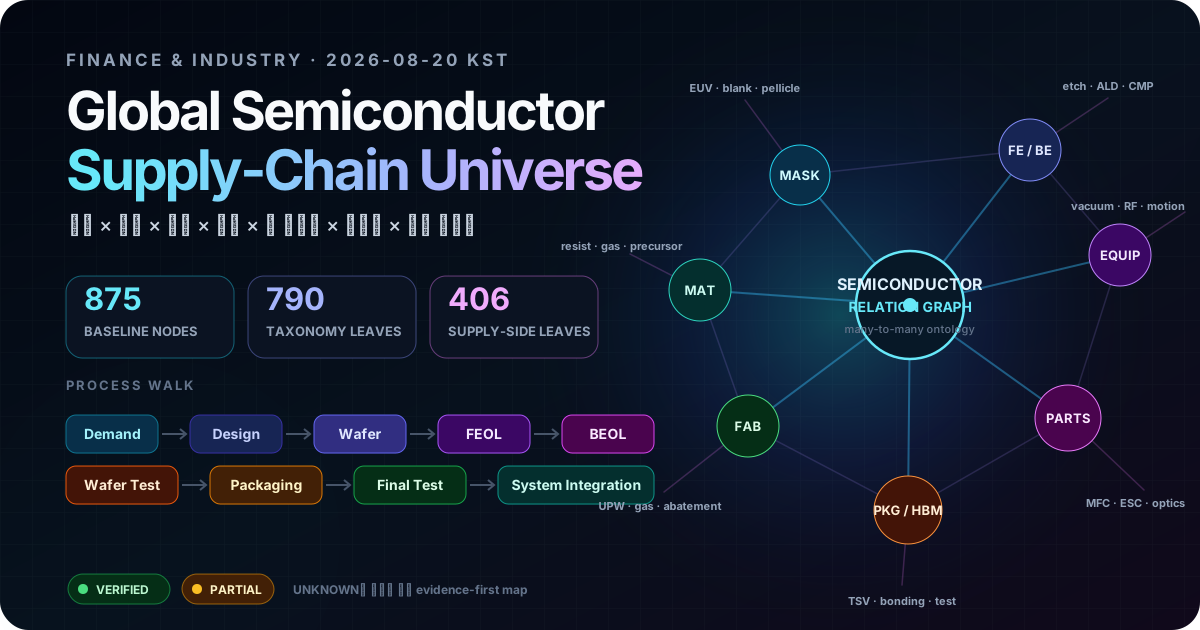
Interactive Relation Atlas
Three.js / WebGPU 기반 반도체 공급망 지도를 전체 화면으로 탐색한다.
Taxonomy, 실제 공정 흐름(Process walk), 기업, 국가, 근거 수준(Evidence)의 다섯 가지 lens를 전환하고, EUV·HBM·MFC·ABF·하이브리드 본딩 같은 node의 upstream/downstream 관계를 추적할 수 있다. WebGPU가 불가능하면 WebGL2로 자동 전환되며, 2D 표와 원본 graph JSON도 함께 제공한다.
Interactive Universe 전체 화면으로 열기 ↗#이 지도는 ‘소부장 목록’이 아니라 산업 운영체계다
반도체를 이해할 때 장비·소재 회사만 따로 모아 보면 중요한 연결을 놓친다. AI 서버 수요가 늘면 먼저 GPU·HBM·네트워크 칩의 사양과 수량이 바뀌고, 그 변화가 설계·마스크·첨단공정·웨이퍼 투입·패키징·테스트의 부담으로 이어진다. 그 뒤에야 lithography, etch, deposition, inspection, gas, chemical, vacuum, RF, substrate, automation, service의 수요가 구체적인 형태로 나타난다.
그래서 이 지도는 회사를 먼저 배열하지 않는다. 아래 다섯 층을 먼저 연결한 뒤, 기업을 각 층의 실제 공급자로 배치한다.
| 읽는 층 | 핵심 질문 | 대표 결과 |
|---|---|---|
| 수요와 제품 | AI·mobile·automotive·industrial 중 어디의 수요가 바뀌는가? | logic·memory·power·sensor의 사양과 물량 |
| 설계와 제조기술 | 어떤 node·architecture·mask·공정 난도가 필요한가? | wafer starts, 공정 단계 수, mask layer, yield learning |
| 생산능력과 운영 | 누가 어떤 fab·back-end capacity를 언제 늘리는가? | capacity, utilization, tool install, service demand |
| 장비·소재·핵심부품 | 어떤 subsystem이 품질·수율·throughput을 제한하는가? | lithography·etch·deposition·inspection, gas·chemical·RF·vacuum·thermal |
| 패키징·테스트·리스크 | die를 어떻게 연결·검증하고, 어느 공급망이 멈추면 전체가 지연되는가? | advanced packaging, HBM, substrate, test, qualification, geography |
이 관점은 주요 산업 리더의 공개 자료와도 맞닿아 있다. TSMC는 foundry를 logic wafer 제조에만 한정하지 않고 mask-making·packaging·testing까지 포함하는 생태계로 설명한다. ASML은 lithography를 장비 판매가 아니라 computational lithography·metrology·system integration·installed-base service를 포함한 해법으로 다룬다. KLA는 wafer·reticle·advanced packaging 전반의 process control을 수율을 지키는 공통 층으로 본다. TSMC Annual Reports · ASML 2025 Annual Report · KLA 2025 Annual Report
처음 읽는 사람을 위한 2분 안내
반도체 공급망을 처음 보면 회사 이름, 장비 이름, 공정 이름이 한꺼번에 나와 어디서 시작해야 할지 막막하다. 이 글은 외울 목록을 늘리기 위한 지도가 아니다. “칩 하나를 만들려면 어떤 일을 하고, 그 일을 하기 위해 어떤 장비·소재·부품이 함께 움직이는가”를 따라가기 위한 지도다.
처음에는 아래 세 질문만 잡으면 충분하다.
- 무엇을 만들고 있는가? — AI 서버용 HBM, 스마트폰용 AP, 자동차용 전력반도체처럼 최종 제품이 다르면 필요한 구조와 공정도 달라진다.
- 웨이퍼 위에서 어떤 변화를 만드는가? — 막을 쌓는 deposition, 도안을 옮기는 lithography, 필요 없는 부분을 깎는 etch, 표면을 평평하게 만드는 CMP가 반복된다.
- 그 변화를 안정적으로 반복하려면 무엇이 필요한가? — 장비 본체만으로는 부족하다. 가스·화학물질, 진공 펌프, RF 전원, 온도 제어, 센서, 로봇, 소모품, 정비가 함께 돌아가야 한다.
그래서 이 글은 회사를 먼저 나열하지 않는다. 최종 수요 → 칩 구조 → 웨이퍼 공정 → 장비 내부 subsystem → 소재·부품 → 검증·서비스 순서로 읽는다. 회사는 이 흐름의 어느 지점에 실제 제품·기술·서비스를 제공하는지 확인할 때 비로소 의미가 생긴다.
#가장 쉬운 출발점: Etcher 한 대를 따라가기
Etcher는 이 지도를 읽는 좋은 출발점이다. 회로의 도안이 웨이퍼에 이미 준비돼 있다고 가정하면, Etcher는 필요 없는 막만 정교하게 제거해 선·구멍·벽을 실제 구조로 만든다. 이 한 장비 안에도 웨이퍼를 옮기는 robot/EFEM, 온도를 맞추는 ESC·chiller, 가스를 계량하는 MFC, 플라즈마를 만드는 RF·matcher, 부산물을 빼는 vacuum pump, 끝점을 판단하는 sensor가 모두 연결된다.
즉 MFC나 pump는 “Etcher 옆에 붙은 작은 부품”이 아니라 결과를 바꾸는 공정 subsystem이다. 이 흐름을 먼저 이해하면 deposition, CMP, scanner, metrology도 같은 방식으로 읽을 수 있다. 인터랙티브 지도에서 Etch부터 열기로 바로 시작할 수 있다.
#웨이퍼 한 장으로 읽는 산업: 공정이 먼저, 기업은 그다음
기업 이름부터 외우면 ASML=노광, Lam=식각처럼 지나치게 단순해진다. 반대로 웨이퍼가 어떤 변화를 거치는지 먼저 보면 각 기업이 왜 연결되는지 자연스럽게 보인다. 실제 양산은 이 순서를 수십·수백 번 반복하고, 검사와 세정은 각 단계 사이에 끼어든다.
수요와 칩 설계 → mask와 패터닝 → 막 형성 → 식각과 구조 형성 → 측정·수율 학습 → 대량 제조 → 패키징·테스트
#1. 수요와 칩 설계 — 무엇을 만들지 정하는 출발점
AI 서버, 스마트폰, 자동차, 산업 장비의 수요는 같은 “반도체 수요”가 아니다. AI 가속기는 연산 칩과 HBM, 빠른 패키지 연결을 요구하고, 자동차 전력반도체는 고전압·고신뢰성 재료와 긴 검증을 요구한다. 제품이 달라지면 회로 구조, 필요한 공정 node, 웨이퍼 수, 패키징 방식도 달라진다.
설계 회사와 IDM은 이 요구를 회로도로 만든다. 다만 설계도는 아직 칩이 아니다. 제조 규칙에 맞게 바꾸고 mask를 만들고, 실제로 수율 있게 생산할 방법까지 정해져야 한다. 이 접점에서 TSMC 같은 foundry가 등장한다. TSMC가 말하는 Foundry 2.0도 wafer 제조만이 아니라 mask-making·packaging·testing까지 포함한다. TSMC 2025 Annual Report
#2. 패터닝 — 빛으로 회로 도안을 웨이퍼 위에 찍는다
패터닝(patterning)은 설계한 회로의 한 층을 웨이퍼에 옮기는 과정이다. 우선 mask에 그려진 도안을 빛으로 photoresist에 비추고, 현상 뒤 남은 resist 모양을 다음 공정의 가이드로 쓴다. 종이에 도장을 찍는 것처럼 보이지만, 선폭이 작아질수록 빛의 회절, mask 오차, 웨이퍼 위치, 앞 공정의 변형이 모두 결과를 바꾼다.
ASML은 이 단계의 scanner를 공급한다. 그러나 중요한 것은 scanner 한 대가 아니라, 원하는 선폭과 층간 정렬(overlay)을 속도와 재현성까지 맞춰 반복하는 체계다. 그래서 computational lithography, mask·resist·pellicle, overlay metrology, 설치 뒤 service와 upgrade가 함께 붙는다. ASML 2025 Annual Report
#3. 막 형성(deposition) — 웨이퍼 위에 다음 구조의 재료를 쌓는다
회로는 한 번에 그려지지 않는다. 절연막, 금속 배선, barrier, transistor의 여러 층을 매우 얇고 균일하게 쌓아야 한다. deposition은 이 막을 형성하는 공정이다. CVD는 기체 반응으로, PVD는 물리적으로, ALD는 한 층씩 표면 반응을 이용해 막을 만든다. 어떤 방법을 쓰느냐에 따라 두께 균일도, 계면 품질, 미세 구조 안쪽까지 덮는 능력(conformality)이 달라진다.
Applied Materials는 이 재료·표면·계면을 다루는 장비를 폭넓게 공급한다. 고객이 평가하는 것은 장비 이름이 아니라 “이 재료가 다음 식각과 전기적 동작까지 견디는가”다. precursor·gas·MFC·showerhead·heater·plasma/RF·vacuum·abatement가 연결되는 이유도 막 한 장의 품질이 이 모든 조건의 결과이기 때문이다. Applied Materials process portfolio
#4. 식각(etch) — 필요 없는 막만 제거해 실제 벽·구멍·통로를 만든다
패터닝으로 resist 도안이 준비되고 막이 쌓였다면, 식각은 그 도안을 따라 필요 없는 부분을 제거한다. 이때 transistor의 gate, 배선이 닿는 contact hole, 3D NAND의 깊은 hole처럼 실제 구조가 만들어진다. 그래서 etch는 “깎는 공정”이면서 회로를 평면 그림에서 3차원 구조로 바꾸는 공정이다.
Lam Research와 Applied Materials는 이 단계의 대표적 장비 공급자다. 건식 식각에서는 가스에 RF 전력을 가해 플라즈마를 만들고, 반응성 입자와 이온으로 원하는 재료를 선택적으로 제거한다. 가스 분포, RF 전력, 진공, 온도, ESC와 edge ring이 조금만 달라져도 깊이·각도·균일도가 달라진다. 따라서 NAND 적층이나 3D logic이 복잡해질수록 etch 장비뿐 아니라 chamber·RF·vacuum·gas delivery 같은 subsystem의 난도도 같이 올라간다. Lam의 plasma etch 기초 설명
#5. 측정과 수율 학습 — 매 단계가 제대로 됐는지 보고 되돌린다
웨이퍼는 패터닝·증착·식각을 한 번만 하지 않는다. 이 묶음을 여러 층에서 반복한다. 작은 결함, 두께 오차, 선폭 오차, 층간 정렬 오차를 늦게 찾으면 이미 여러 단계의 웨이퍼가 손실될 수 있다. inspection은 결함을 찾고, metrology는 선폭·두께·overlay처럼 숫자로 관리해야 하는 값을 잰다.
KLA는 이 공정 제어(process control) 층의 대표 기업이다. 역할은 완성품 불량을 골라내는 데서 끝나지 않는다. 어느 장비·recipe·재료 조건을 고쳐야 수율이 회복되는지 학습할 데이터를 제공한다. 그래서 검사·계측은 전공정뿐 아니라 mask와 advanced packaging에도 이어진다. KLA FY2025 Annual Report
#6. 대량 제조와 패키징 — 작동하는 칩을 시스템 부품으로 완성한다
이 모든 공정을 안정적으로 반복해 양산하는 곳이 fab이다. TSMC 같은 foundry는 고객 설계를 받아 웨이퍼 투입, 공정 운전, 수율 안정화, 출하를 관리한다. 여기서 생산능력은 건물 크기만이 아니다. 검증된 tool 조합, 숙련된 운영, utilities, 공급망, service, 실제 가동률이 함께 만든 capacity다.
웨이퍼가 완성되면 칩을 분리하고, 기판 위에 연결하고, 열을 빼고, 전기적으로 검사한다. HBM이나 chiplet에서는 여러 die를 패키지 안에서 연결하는 단계가 성능과 공급 병목을 좌우한다. TSMC는 첨단 패키징을 foundry 생태계의 일부로 다루고, KLA는 패키지 검사·계측에도 연결된다. 따라서 “웨이퍼 제조가 끝났으니 반도체가 끝났다”가 아니라, 패키징·테스트를 통과해 시스템에 들어갈 때 비로소 제품이 된다.
#기업을 공정 위에 다시 놓으면
TSMC는 설계와 fab 운영·첨단 패키징을 연결한다. ASML은 도안을 정확히 찍는 패터닝을 담당한다. Applied Materials는 막과 재료를 다루는 층에서 넓게 연결되고, Lam은 복잡한 구조를 만드는 식각·증착·세정에 강하게 연결된다. KLA는 이 모든 단계의 결과를 보고 수율 학습으로 되돌린다. 이제 기업을 독립 목록이 아니라, 웨이퍼를 따라가는 각 공정의 공급자와 운영자로 읽을 수 있다.
#먼저 읽어야 할 결론
이 연구의 핵심은 “유명 반도체 기업을 많이 찾는 것”이 아니다. 독립적인 procurement market, qualification stack, unit-process function을 형성하는 최소 단위를 leaf node로 등록하고, 그 node를 실제 제조공정과 공급기업에 연결하는 것이다.
Phase 1에서 구축한 baseline은 875개 node, 790개 leaf node다. 이 중 공급기업 census의 직접 대상이 되는 supply-side leaf는 Phase 2에서 406개로 재구성했다. 그러나 이 숫자는 모든 node의 시장점유율, 고객 qualification, 한국 기업의 HVM(High-Volume Manufacturing) 공급 여부까지 완성됐다는 뜻이 아니다.
현재 공개 Atlas는 다음 두 사실을 동시에 보존한다.
- Taxonomy topology: 무엇이 어디에 속하고 어떤 공정·장비·소재·부품과 연결되는지 보여준다.
- Evidence status: 충분히 확인된 것은
VERIFIED, 일부만 확인된 것은PARTIAL로 구분한다. 확인되지 않은 고객관계와 시장점유율을 임의로 채우지 않는다.
따라서 이 페이지는 “완성됐다고 선언한 종목지도”가 아니라, 지속적으로 증거를 붙여 나가는 semiconductor research database의 public interface다.
#왜 tree가 아니라 graph인가
반도체 공급망은 하나의 회사가 하나의 category에만 속하는 tree가 아니다.
예를 들어 Applied Materials는 deposition만 하는 회사가 아니라 ALD/CVD/PVD/ECD, etch, CMP, implant, metrology, photomask, hybrid bonding과 compound/power semiconductor까지 여러 node에 걸친다. ASML도 scanner만이 아니라 computational lithography, metrology, inspection ecosystem과 연결된다. 한국의 FST 역시 pellicle뿐 아니라 EUV pellicle handling/inspection, SiC chamber parts, scrubber와 chiller에 걸친다.
그래서 database 구조는 다음 many-to-many 관계를 허용해야 한다.
Supplier ↔ Material / Equipment / Component / Service
Equipment ↔ Subsystem / Consumable / Utility
Process ↔ Material / Equipment / Metrology / Software
Device architecture ↔ Process intensity
End market ↔ Product demand ↔ Manufacturing demand
이 원칙이 없으면 “ASML=노광장비”, “OSAT=패키징”, “소부장=대형 장비회사” 같은 지나친 축약이 발생한다.
#1. 반도체 Supply-Chain Topology: 지도에 무엇이 들어 있는가
이 지도는 회사 목록이 아니라, 하나의 반도체가 수요에서 출발해 설계·제조·패키징·검증을 거쳐 시스템에 들어갈 때 필요한 산업 층을 함께 놓은 topology다. 왼쪽의 수요가 제품의 사양과 물량을 만들고, 중간의 설계·웨이퍼·공정이 칩을 만들며, 오른쪽의 패키징·테스트가 사용할 수 있는 부품으로 완성한다. 소재·장비·핵심부품·팹 인프라·자동화는 그 흐름 전체를 가로지르는 공통 기반이다.
| 산업 층 | 포함 영역 | 이 지도를 읽을 때의 질문 |
|---|---|---|
| 수요·제품 | DEM: AI/HPC·server·mobile·automotive 등 / PROD: DRAM·HBM·NAND·CPU·GPU·power·sensor 등 | 누가 어떤 칩을 얼마나 필요로 하는가? |
| 설계·원판 준비 | DESIGN: IDM·fabless·foundry·EDA·IP / WAF: silicon·SOI·SiC·GaN·epi / MASK: blank·reticle·pellicle·inspection | 그 칩을 만들 도안과 출발 재료는 무엇인가? |
| 웨이퍼 제조·공정 제어 | FE: clean·lithography·etch·deposition·implant·CMP·metallization / PC: inspection·overlay·CD·yield·APC | 웨이퍼 위에 구조를 어떻게 만들고, 제대로 만들어졌는지 어떻게 확인하는가? |
| 소재·장비·핵심부품 | MAT: resist·gas·chemical·precursor·CMP·chamber material / EQCOMP: vacuum·RF·gas delivery·chamber·motion·optics·thermal·robotics·sensor | 공정 결과를 실제로 바꾸는 소모재와 장비 subsystem은 무엇인가? |
| 공장 운영 기반 | FAB: cleanroom·UPW·gas·chemical·abatement·cooling·power / AUTO: AMHS·FOUP·MES·FDC·APC·cybersecurity | 수천 장의 웨이퍼를 오염 없이, 같은 조건으로 반복 생산하려면 무엇이 필요한가? |
| 완성·검증·순환 | PKG: thinning·bump·TCB·hybrid bonding·RDL·TSV / TEST: probe·ATE·burn-in·reliability / HBM·SERVICE | 칩을 연결·보호·검증하고, 장비를 유지·복원하는 마지막 단계는 무엇인가? |
#2. Wafer를 따라가는 제조 흐름
Taxonomy가 실제 제조흐름과 연결되는지 확인하기 위해 wafer 한 장이 공장을 통과한다고 가정했다.
| 흐름 | 웨이퍼·다이에 일어나는 변화 | 함께 봐야 할 공급망 |
|---|---|---|
| 1. 출발 재료 | silicon·SiC·GaN 등을 고순도 웨이퍼로 만든다 | ingot·epi·polishing·clean·substrate 검사 |
| 2. 도안 준비 | 회로 설계 데이터를 reticle로 옮긴다 | EDA·mask blank·writer·pellicle·mask inspection |
| 3. 전공정 | 막을 쌓고, 빛으로 도안을 옮기고, 필요한 부분을 깎아 transistor와 배선을 만든다 | deposition·lithography·etch·implant·CMP + gas·resist·vacuum·RF·metrology |
| 4. 웨이퍼 검사 | die가 전기적으로 동작하는지 판별해 KGD 후보를 고른다 | probe card·tester·inspection·yield analysis |
| 5. 패키징 | 웨이퍼를 얇게 만들고 절단한 뒤, 다른 die와 연결·보호한다 | dicing·substrate·bump·TCB·hybrid bonding·molding·thermal |
| 6. 최종 검증·시스템 | 완성품의 성능·신뢰성을 검증하고 서버·모바일·자동차 시스템에 탑재한다 | ATE·handler·burn-in·socket·SLT·reliability |
한 줄로 보면: 수요 → 칩 사양 → 설계·마스크 → 웨이퍼 전공정 → 웨이퍼 검사 → 패키징 → 최종 테스트 → 시스템. 소재·장비·핵심부품·공장 인프라는 이 모든 화살표에 반복해서 붙는다.
각 step마다 장비만 묻지 않았다. 다음 열 가지를 반복해서 확인했다.
- Equipment
- Material
- Consumable
- Critical component
- Gas / chemical
- Contamination control
- Metrology / inspection
- Wafer handling
- Utility / facility
- Maintenance / service
이 방식으로 일반적인 “8대 공정” 설명에서 빠지는 post-etch clean, edge/bevel, descum, temporary bonding/debonding, chemical/gas inline analytics, carrier cleaning, calibration, refurbishment가 독립 node로 드러났다.
#3. 장비 핵심부품: 장비 한 대 안에서 실제로 공정을 만드는 것
반도체 산업지도를 만들 때 가장 자주 빠지는 부분은 장비 OEM이 아니라 장비 내부 critical subsystem이다.
Etcher는 대표 사례일 뿐, 이 표의 읽는 법은 scanner·deposition·CMP·clean 장비에도 그대로 적용된다.
| Etcher subsystem | 대표 부품 | 공정에서 하는 일 | 흔들리면 나타나는 문제 |
|---|---|---|---|
| 반응 공간 | chamber body·liner·coating·quartz·ceramic·SiC·seals | 반응을 가두고 내부 표면을 보호한다 | particle·부식·공정 편차 |
| 플라즈마·전력 | plasma source·RF generator·matcher·power supply | 가스를 반응성 있는 플라즈마로 만들고 안정적으로 에너지를 전달한다 | 식각 모양·반복성 저하 |
| 고정·열 관리 | ESC·electrode·edge/focus ring·chiller·heater | 웨이퍼 위치와 온도를 일정하게 유지한다 | 중심/가장자리 불균일 |
| 가스 전달 | purifier·regulator·valve·MFC·showerhead | 순도·압력·유량·분포를 맞춘다 | 반응 조성·균일도 변화 |
| 진공·배출 | dry/turbo pump·gauge | 압력과 부산물 배출 조건을 만든다 | 압력 응답·오염·잔류 부산물 |
| 이송·자동화 | load port·EFEM·robot | 웨이퍼를 오염 없이 정확히 옮긴다 | particle·정렬·처리량 문제 |
사례로 더 보기: Etcher가 공정을 만드는 방식
#Etcher는 무엇을 하는 장비인가
Etcher(식각 장비)는 웨이퍼 위에 이미 쌓인 얇은 막에서, 회로가 필요하지 않은 부분만 골라 제거하는 장비다. 비유하면 사진 현상 뒤 남은 도안을 따라 돌을 깎는 조각 도구에 가깝다. 빛으로 도안을 옮기는 장비가 노광기라면, Etcher는 그 도안을 실제 3차원 구조로 바꾸는 장비다. Samsung의 식각 기초 설명과 Applied Materials의 etch 개요에서 먼저 큰 그림을 볼 수 있다.
건식 식각에서는 가스를 진공 챔버에 넣고 RF 전력을 가해 플라즈마를 만든다. 플라즈마 안의 라디칼은 재료와 화학 반응을 일으키고, 이온은 아래 방향으로 에너지를 전달해 바닥을 더 잘 깎게 한다. 반응 뒤 생긴 휘발성 부산물은 진공계가 밖으로 빼낸다. 즉, Etcher는 단순히 “가스를 뿌리는 기계”가 아니라 가스·전기장·온도·압력·이송을 동시에 맞춰 원하는 모양을 만드는 시스템이다. Lam Research의 plasma etch 원리에서 화학 반응과 이온 충돌이 함께 작동하는 이유를 확인할 수 있다.
#공정 안에서 보는 5단계
-
웨이퍼를 넣는다 — Robot / EFEM / load port
FOUP에서 웨이퍼를 꺼내 장비 안으로 옮기고, 방향과 위치를 맞춘다. 여기서의 작은 오염이나 정렬 오류도 뒤 공정의 결함으로 이어질 수 있다. EFEM·load port·robot 예시
-
웨이퍼를 고정하고 온도를 맞춘다 — ESC / edge ring / chiller
ESC(electrostatic chuck)는 정전기로 웨이퍼를 붙잡는 척이다. 뒷면 헬륨과 chiller가 열을 빼 온도를 일정하게 유지한다. 온도가 달라지면 식각 속도와 옆면 모양이 함께 바뀐다. ESC의 역할 · 반도체 chiller 예시
-
정확한 양의 가스를 보낸다 — purifier / regulator / valve / MFC / showerhead
Purifier는 불순물을 줄이고, regulator·valve는 압력과 흐름을 제어하며, MFC(mass flow controller)는 가스 유량을 정밀하게 계량한다. Showerhead는 가스를 웨이퍼 위에 고르게 분배한다. 같은 가스라도 유량과 분포가 달라지면 웨이퍼 안쪽과 바깥쪽의 결과가 달라질 수 있다. MFC 기초 제품 자료
-
플라즈마로 필요한 부분만 제거한다 — plasma source / RF generator / matcher
RF generator가 전력을 만들고, matcher가 챔버의 전기적 상태에 맞춰 그 전력이 잘 전달되게 조정한다. 이렇게 생긴 플라즈마의 이온·라디칼이 마스크로 보호되지 않은 부분을 제거한다. 여기서 중요한 결과는 ‘얼마나 빨리 깎는가’만이 아니다. 아래 방향으로 곧게 깎이는지(방향성), 다른 막은 남기는지(선택비), 웨이퍼 전체가 같은 결과인지(균일도)를 함께 본다. RF power와 match network의 역할
-
부산물을 빼고 결과를 확인한다 — chamber liner / coating / dry·turbo pump / gauge / endpoint sensor
챔버 안벽과 liner는 플라즈마·부식·파티클을 견디고, 펌프와 밸브는 압력과 부산물 배출을 관리한다. 센서는 원하는 막이 제거된 순간을 판단하는 데 쓰인다. 그래서 부품 하나를 교체해도 단순 수리로 끝나지 않고, 파티클·압력 응답·RF 조건·수율을 다시 검증해야 한다. 반도체 dry pump 설명 · endpoint monitoring 예시
#목록을 공급망으로 읽는 법
아래 부품은 서로 독립된 체크리스트가 아니다. 가스 공급 → 플라즈마 생성 → 웨이퍼 위 반응 → 부산물 배출 → 센서 피드백이라는 하나의 폐루프다. 예를 들어 MFC가 흔들리면 가스 조성이 바뀌고, plasma/RF 조건과 식각 모양이 달라질 수 있다. ESC·chiller가 흔들리면 웨이퍼 온도가 바뀌며 선택비·균일도에 영향을 준다. pump·valve·liner가 나빠지면 압력이나 오염 상태가 달라져 같은 recipe라도 다른 결과가 날 수 있다.
인터랙티브 지도에서는 Etch 공정부터 열기한 뒤, MFC, Plasma / RF, ESC, Vacuum Pump, Robot / EFEM 노드를 차례로 선택하면 각 항목의 공식 기술 링크를 확인할 수 있다.
#같은 틀로 보는 Scanner
Scanner는 회로 도안을 웨이퍼에 빛으로 옮기는 노광 장비다. Light source는 필요한 파장의 빛을 만들고, optics는 그 빛을 정밀하게 다룬다. Stage는 reticle과 wafer를 매우 정확하게 움직이며, encoder는 그 위치를 읽는다. Vibration isolation은 미세한 흔들림이 패턴 오차로 번지는 것을 막는다. Reticle handling과 wafer handling은 마스크와 웨이퍼를 오염 없이 이송하고, sensor와 overlay metrology는 새로 찍힌 층이 이전 층과 얼마나 정확하게 맞았는지 확인한다.
그래서 Scanner 공급망을 볼 때는 광원 회사나 렌즈만 보는 것으로 끝나지 않는다. 정밀 motion, position encoder, 진동 제어, reticle pod·handling, wafer stage, overlay 계측까지 함께 봐야 한다. 한 층의 위치가 조금만 어긋나도 수많은 회로 층이 쌓인 뒤에는 연결 불량이나 수율 저하로 이어질 수 있기 때문이다.
#같은 틀로 보는 Deposition
Deposition tool은 웨이퍼 위에 금속·절연막·barrier·liner 같은 얇은 막을 필요한 두께와 균일도로 쌓는다. 이를 위해 precursor delivery가 반응 재료를 공급하고, vaporizer는 액체 전구체를 기체 상태로 바꾸며, MFC·valve·showerhead가 전달량과 분포를 제어한다. Heater는 반응에 필요한 온도를 만들고, plasma/RF는 일부 공정에서 반응성을 높인다. Pump는 쓰고 남은 가스와 부산물을 빼며, abatement는 유해 배출가스를 처리한다.
따라서 deposition 장비의 성능은 ‘막을 만들 수 있는가’가 아니라, 웨이퍼 전체에 같은 막을 만들 수 있는지, 아주 좁고 깊은 구조 안쪽까지 막을 넣을 수 있는지, 불순물과 파티클을 관리하는지에 달려 있다. Etcher와 마찬가지로 gas delivery, thermal control, vacuum, plasma, chamber material이 하나의 연결된 시스템을 이룬다.
#장비 핵심부품의 진입장벽: 재검증
반도체 장비의 부품 교체는 일반 설비의 소모품 교체와 다르다. 새 부품이 들어가면 파티클 발생, plasma uniformity, thermal stability, outgassing, corrosion resistance, RF impedance, pressure response가 조금씩 달라질 수 있다. 각 항목은 영어 그대로 쓰더라도 결국 같은 질문으로 돌아온다. “이 부품을 바꾼 뒤에도 웨이퍼가 전과 같은 모양과 전기적 특성으로 나오는가?”
그래서 장비 회사와 팹은 tool-level requalification과 wafer yield validation을 거친다. 먼저 장비 조건이 안정적으로 재현되는지 확인하고, 그 다음 실제 웨이퍼에서 결함·치수·전기 특성·수율이 기존 수준을 유지하는지 본다. 이 과정이 길고 고객별 recipe가 다르기 때문에 설치대수(Installed base), qualification 기간, 현장 서비스 network가 장비 핵심부품 시장의 진입장벽이 된다. 단지 부품을 만들 수 있는지보다, 이미 돌아가는 수많은 장비에서 신뢰성 있게 교체되고 검증될 수 있는지가 더 중요하다.
#Materials Chemistry: “가스·화학” 한 줄로 끝내지 않는다
Materials universe도 broad category만으로는 부족하다.
- Lithography: KrF/ArF/ArFi/EUV resist, developer, thinner, BARC, topcoat, HMDS, EBR chemical
- Wet process: H₂SO₄, H₂O₂, HF, HNO₃, HCl, H₃PO₄, NH₃, IPA와 ultra-high-purity solvents
- Etch/clean gases: fluorocarbon, chlorine, bromine, NF₃, F₂, remote-plasma clean chemistry
- Deposition: ALD/CVD metal·high-k·barrier/liner precursor, carrier/purge gas
- Implant/doping: boron, phosphorus, arsenic 계열 dopant gas/source
- CMP: slurry, pad, conditioner, post-CMP clean chemistry
- Plating: Cu chemistry, suppressor, accelerator, leveler, electroless chemistry
- Chamber consumables: quartz, alumina, AlN, Y₂O₃ coating, SiC, graphite, elastomer seals
- Packaging: ABF, BT resin, EMC, underfill, NCF/NCP, die attach, TIM, flux, solder/bump materials
같은 화학명이라도 semiconductor grade의 금속불순물, particle, moisture, delivery stability와 container/valve cleanliness가 다르면 별도 qualification market이 된다.
#HBM은 DRAM만이 아니라 복합 manufacturing graph다
HBM 공급망은 다음과 같이 연결된다.
AI accelerator demand
→ Advanced DRAM wafer
→ Wafer test / Known Good Die
→ TSV etch + liner/barrier/seed + Cu plating + CMP
→ Wafer thinning / stress relief / reveal
→ Microbump·Cu pillar 또는 hybrid interface
→ High-accuracy placement + TCB / bonding
→ MR-MUF·NCF·molding
→ Logic base die + interposer/RDL + package substrate
→ TIM / heat spreader / warpage control
→ Final test / burn-in / high-speed thermal test
HBM4에서 중요한 변화는 bandwidth 숫자만이 아니다. 더 많은 I/O, logic base die, 더 높은 stack/package complexity, thermal·power integrity와 test difficulty가 함께 증가한다. 따라서 HBM 수요의 전달경로는 다음과 같이 분석해야 한다.
AI server
→ GPU / accelerator shipments and HBM bytes per accelerator
→ Advanced DRAM wafer demand
→ TSV / thinning / bonding step intensity
→ Interposer / substrate / thermal complexity
→ Probe / KGD / package test value per package
→ Equipment, material, component and service revenue exposure
HBM4 mass production, HBM4E sample/qualification, future HBM roadmap은 동일한 상태가 아니다. 또한 hybrid bonding을 모든 HBM4 제품의 현재 표준으로 일반화하지 않는다.
#Technology inflection이 산업 공급망에 전달되는 경로
#GAA / Nanosheet
3D gate/channel geometry는 conformal ALD, selective epi, selective/isotropic etch, interface control과 3D metrology의 공정강도(Process intensity)를 높인다.
#Backside Power Delivery
Front-side routing만 바뀌는 것이 아니다. temporary bonding, extreme thinning, backside alignment, via etch, dielectric/metal deposition, lithography, CMP와 backside inspection이 새로 연결된다.
#High-NA EUV
High-NA는 scanner-only market이 아니다. source·optics·stage뿐 아니라 mask, pellicle, resist/underlayer, track defectivity, stochastic control, overlay와 actinic inspection까지 하나의 qualification ecosystem을 형성한다.
#Hybrid Bonding
Bond pitch가 줄어들수록 surface roughness와 planarity tolerance가 작아지고, CMP, ultra-clean surface preparation, plasma activation, sub-micron alignment, interface metrology와 KGD의 중요도가 커진다.
#Chiplet / UCIe
Die 수와 die-to-die interface가 늘어나면 package co-design, RDL/interposer/substrate, placement/bonding, SI/PI validation과 partitioned test가 복잡해진다.
#SiC / GaN
기판결함, epi quality, high-temperature process, backside metal, wafer handling과 specialty inspection이 silicon CMOS와 다른 독립 flow를 만든다.
#구조적 Chokepoint
공개자료만으로 최신 세부 시장점유율을 확정할 수 없는 node에는 임의의 숫자를 넣지 않았다. 대신 concentration, qualification, replacement time, 기술장벽과 geographic concentration을 결합해 구조적 병목 후보를 구분했다.
| Chokepoint family | 병목이 생기는 이유 |
|---|---|
| EUV / High-NA scanner–optics–source | 극단적 광학·광원·motion integration, 제한된 공급기반, 장기간 공동 qualification |
| Advanced mask ecosystem | EUV blank, multi-beam writing, blank/actinic inspection, pellicle의 상호의존성 |
| Leading-edge process control | defect size 축소와 3D 구조 때문에 inspection/metrology 없이는 yield learning 불가능 |
| ABF / high-end substrate | package density 증가, long qualification, build-up substrate 공정 복잡성 |
| ATE / probe / high-speed test interface | AI/HBM I/O와 power 증가로 test coverage·signal integrity·thermal 요구 동시 상승 |
| Tool critical components | MFC, valve, purifier, RF, ESC, pump/abatement 교체가 tool/process 재검증으로 연결 |
| Ultra-high-purity chemistry | contamination excursion이 여러 lot의 yield loss로 확대될 수 있음 |
#한국 반도체 공급망 지도
한국은 메모리 제조 외에도 silicon wafer, specialty gas, 일부 photoresist/process chemicals, dry strip, deposition/clean, high-pressure anneal, scrubber/chiller, cleanroom/FFU, chamber consumables, FCBGA와 test interface에서 의미 있는 공급자층을 형성했다.
그러나 국산화 제품 존재와 leading-edge HVM qualification은 다르다.
| Node | 2026-08-20 판정 |
|---|---|
| Silicon / selected SiC wafer | 글로벌 경쟁 가능 |
| DUV resist, wet chemicals, NF₃/WF₆ | 국내·글로벌 경쟁 공급자 존재 |
| Selected deposition/clean/dry strip/HPA tools | 경쟁력 보유, node별 격차 상이 |
| Quartz/Si/SiC chamber parts | 상당 부분 국내 경쟁 가능 |
| Scrubber/chiller, cleanroom/FFU, AMHS | 국내 ecosystem 강함 |
| FCBGA, sockets/pins/test interfaces | 글로벌 경쟁 node 존재 |
| EUV scanner, High-NA optics/source | 사실상 수입 chokepoint |
| Advanced mask blank / actinic inspection | 해외 의존 높음 |
| Leading optical/e-beam process control | 해외 의존 높음 |
| Leading-edge ion implant / high-end ATE | 해외 의존 높음 |
| ABF | 매우 높은 해외 의존 |
| Hybrid bonding | application별 development/qualification 단계가 다름 |
특히 상장사만 보면 놓치는 long-tail이 있다. FST, Value Engineering, Seojin Electron, DeviceEng, CanTops, LSE, SUNJE, MMT, MMP, 3SLINE, Gauss Labs, Woowon Technology, Semics 등은 component, carrier cleaning, AMHS interface, utility monitoring, technical representation, wafer test 같은 leaf에서 다시 확인해야 한다. 다만 exhibitor와 product page는 제품 존재의 증거이지 삼성전자·SK hynix HVM 공급의 증거가 아니다. 고객관계가 공식적으로 확인되지 않으면 UNVERIFIED로 둔다.
#국가별 구조적 강점
| Region | 주요 강점 node |
|---|---|
| United States | EDA/IP, deposition/etch/implant, process control, ATE, AI compute |
| Korea | DRAM/HBM/NAND, memory HVM, specialty gases·chemicals, selected equipment/components/test |
| Taiwan | leading foundry, advanced packaging, substrate ecosystem |
| Japan | wafer, resist, mask blank, high-purity chemicals, CMP, clean, dicing/test equipment |
| Netherlands | lithography, deposition, advanced bonding |
| Germany | EUV optics/laser, specialty materials/equipment |
| France | industrial/specialty gases, SOI ecosystem |
| China | mature-node expansion과 aggressive domestic localization; advanced-tool export-control exposure |
| Singapore / Malaysia / Vietnam | supplier manufacturing hubs, OSAT/test, downstream electronics·packaging expansion |
| India | design talent와 fab/ATMP build-out |
| Israel | specialty process, metrology/inspection R&D |
여기서 “장비를 누가 만드는가”와 “장비가 어느 국가의 fab으로 배송되는가”는 다른 geography layer다.
#시장규모: 서로 다른 TAM을 합산하지 않는다
시장 숫자는 정의와 시점을 함께 표시해야 한다.
| Metric | Data period | Status | Value |
|---|---|---|---|
| Semiconductor equipment billings | 2025 | Actual | $135B |
| Total semiconductor manufacturing equipment | 2026 | Forecast | $165.9B |
| Wafer Fab Equipment | 2026 | Forecast | $143.9B |
| Test equipment | 2026 | Forecast | $15.3B |
| Assembly / packaging equipment | 2026 | Forecast | $6.7B |
| Semiconductor materials | 2025 | Actual | $73.2B |
| Wafer-fab materials | 2025 | Actual | $45.8B |
| Packaging materials | 2025 | Actual | $27.4B |
| Semiconductor device market | 2026 | Forecast | $1.51T |
마지막 device market는 chip sales다. equipment, materials와 포함관계가 다르므로 소부장 TAM과 더해서 “전체 반도체 시장”이라고 부르지 않는다. Fab equipment spending과 equipment billings도 정의가 다르다.
#Evidence discipline
이 지도에서 고객관계는 다음 상태를 구분한다.
Rumor
→ Evaluation
→ Sample shipment
→ Qualification
→ Production qualification
→ Initial mass production
→ High-volume manufacturing
→ Long-term supply agreement
“삼성전자에 공급할 것으로 예상된다”와 “삼성전자 양산라인에 공급 중”은 같은 문장이 아니다. 고객사·공급사 공식자료, 공시 또는 계약자료로 확인되지 않으면 UNVERIFIED다.
주요 claim의 evidence grade도 분리한다.
- A: Primary source + independent corroboration
- B: Primary source only
- C: High-quality secondary source
- D: Company marketing claim only
- E: Rumor / weak evidence
D/E는 핵심 결론의 근거로 사용하지 않는다.
#현재 Atlas가 보여주는 것과 아직 보여주지 못하는 것
Interactive Atlas에는 audited topology, 주요 공정 node, equipment-component dependency, 대표적인 global/Korean supplier anchor와 일부 공식 customer relation을 넣었다. 현재 공개 graph는 322 nodes, 611 relations를 렌더링한다.
그러나 다음은 계속 PARTIAL 또는 UNKNOWN으로 남는다.
- 790개 모든 leaf의 최신 global supplier share
- 세부 market의 2025/2026 TAM과 CAGR
- Korean long-tail supplier의 고객별 evaluation/qualification/HVM 단계
- China domestic replacement map의 leaf-level completeness
- High-NA의 foundry별·layer별 production adoption
- HBM generation별 bonding process-of-record
- company legal entity와 subsidiary 단위의 완전한 many-to-many revenue mapping
이 미확인 영역을 숨기지 않는 것이 이 연구의 핵심 품질조건이다.
#Interactive Atlas 사용법
- Taxonomy lens: 15개 상위 domain과 하위 node의 계층을 본다.
- Process lens: wafer가 manufacturing flow를 통과하는 순서로 재배치한다.
- Company lens: supplier와 buyer/platform anchor를 중심으로 본다.
- Geography lens: 공급망 강점과 geographic dependency를 본다.
- Evidence lens: VERIFIED/PARTIAL과 evidence grade 차이를 본다.
- Incoming / Outgoing trace: 선택 node의 upstream/downstream relation을 강조한다.
- Search: Node ID, 공정, 소재, 부품, 기업명으로 이동한다.
- 2D table: GPU를 쓰지 않고도 동일 graph를 검색한다.
#Primary source registry
아래는 이 공개판의 시장·기술상태·taxonomy anchor에 사용한 주요 primary source다.
- SEMI — Semiconductor Equipment Market Data
- SEMI — 2025 Semiconductor Materials Market, $73.2B
- SEMI — Semiconductor Components, Instruments and Subsystems
- SEMICON Korea — Exhibitor and category structure
- WSTS — 2026 global semiconductor market forecast
- ASML — High-NA EUV readiness milestone
- Intel Foundry — Intel 18A, RibbonFET and PowerVia
- SK hynix — HBM4 development and mass-production readiness
- Micron — HBM4 high-volume production
- U.S. BIS — Export-control changes for foreign-owned fabs in China
- 산업통상자원부 — 반도체 소부장·미니팹·첨단패키징 관련 공고
#다음 업데이트 기준
이 map은 고정된 이미지가 아니라 versioned research asset으로 관리한다. 다음 업데이트에서는 다음 세 가지를 우선한다.
- 790개 leaf와 406개 supply-side leaf를 machine-readable ledger로 직접 연결한다.
- supplier–customer edge에 evaluation/qualification/HVM과 source date를 강제한다.
- 각 node의 TAM, market definition, actual/estimate/forecast를 분리한 source registry를 확장한다.
최종 목표는 UNKNOWN을 억지로 없애는 것이 아니다. 무엇을 알고, 어떤 관계가 검증됐고, 어디부터 다시 조사해야 하는지를 보존하는 것이다.